
Official websites use .gov
A .gov website belongs to an official government organization in the United States.
Secure .gov websites use HTTPS
A lock (
) or https:// means you’ve safely connected to the .gov website. Share sensitive information only on official, secure websites.
GlobalWafers (Missouri)
Key Facts
Project Summary
The U.S. Department of Commerce made direct funding awards to GlobalWafers America, LLC (GWA) and MEMC LLC (MEMC), subsidiaries of GlobalWafers Co., Ltd. (GlobalWafers), of up to $406 million to support the construction of new wafer manufacturing facilities in Sherman, Texas and St. Peters, Missouri.
Economic And National Security Impact
Silicon wafers, which will be produced by GWA in Sherman, Texas, are foundational components in the semiconductor ecosystems, serving as essential inputs for all chips, including leading-edge, mature-node, and memory chips. Approximately 90% of silicon wafers are sourced from East Asia today, with five corporations managing the majority of global supply – GlobalWafers is one of the five global leaders in this market. Accordingly, by supporting this facility, the U.S. is taking a meaningful step to strengthen supply chain resilience and help support a reliable domestic supply of key semiconductor components.
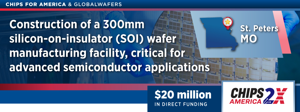
Silicon-on-Insulator (SOI) wafers, which will be produced by MEMC in St. Peters, Missouri, are critical for advanced semiconductor applications as they enable higher performance, lower power consumption, and improved thermal efficiency, making them essential for cutting-edge technologies in defense, aerospace, and high-performance computing. SOI wafers can also be made to feature radiation-hardened characteristics, which are critical for semiconductor performance and reliability for several defense and aerospace end uses. This project will serve as the key domestic site for 300mm SOI wafers in the U.S., helping to advance U.S. economic and national security by significantly expanding domestic capacity and technological capabilities.
Finally, as part of the award agreement, GlobalWafers has agreed to convert a portion of its existing silicon epitaxy wafer manufacturing facility in Sherman, Texas to silicon carbide (SiC) epitaxy wafer manufacturing, producing 150mm and 200mm SiC epitaxy wafers. SiC epitaxy wafers are a critical component for high-voltage applications, notably including electric vehicles and clean energy infrastructure.
Workforce and Community Impact
Through GlobalWafers’ construction and manufacturing operations, this investment is expected to support approximately 1,700 construction jobs and 880 manufacturing jobs across Texas and Missouri.
To recruit, train, and retain the workforce needed for these projects, GlobalWafers will implement a robust workforce strategy informed by the Biden-Harris Administration’s Good Jobs Principles and will receive up to $6 million in dedicated CHIPS funding to implement workforce initiatives including worker recruitment and training.
To advance its manufacturing workforce efforts:
- In Texas, GlobalWafers is a member of the Southern Methodist University-led Texoma Tech Hub and participates in the North Texas Semiconductor Workforce Development Consortium led by the University of Texas Dallas.
- GlobalWafers is also part of an innovative partnership with Sherman High School, Denison High School, and Grayson College to establish an electronics lab at the schools that provide targeted training towards technician certifications required for new hires in the semiconductor industry.
- In Missouri, MEMC is likewise developing an apprenticeship program for Maintenance Technicians with the National Institute for Industry and Career Advancement (NIICA) and local high schools.
- MEMC is collaborating with St. Charles Community College on a program named MegaTech, which supports dual-enrolled high school students as they step into careers involving advanced manufacturing and automation.
Environmental and Worker Safety Commitments
In connection with the CHIPS award, the Department is requiring GlobalWafers to commit to the following environmental responsibility and worker safety measures in its operations. As is required for all CHIPS projects, the GlobalWafers projects will comply with all applicable environmental laws, including the Clean Water Act, Clean Air Act, Endangered Species Protection Act, and the Resource Conservation and Recovery Act.
In connection with the CHIPS award, GlobalWafers is making the following environmental commitments:
- Carbon-Free Electricity: By the end of the decade, GlobalWafers will use commercially reasonable efforts to operate the project with 100% carbon-free electricity.
- Water: Within one year of completing the project, GlobalWafers will use commercially reasonable efforts to recycle at least 50% of the process water used onsite.
- Public Reporting: GlobalWafers will report the environmental responsibility goals it has adopted and disclose annual progress toward those environmental goals, including:
- energy (kWh) used, saved through conservation programs, and produced from clean energy sources;
- water used, conserved, and recycled; and
- total waste generated and percentage total hazardous and nonhazardous waste destined for a landfill, incinerator, recycling facility, or treatment facility.
GlobalWafers has also committed to the following worker safety measures:
- Worker Safety Committee: GlobalWafers will establish or maintain a workplace safety committee comprised of workers and management that meets regularly and is authorized to address any worker health and safety concerns.
- Adoption of Most Protective Occupational Exposure Limits: GlobalWafers will apply the lowest (i.e., most protective) occupational exposure limit (OEL) among all applicable published health and safety standards (including National Institute for Occupational Safety and Health and American Conference of Governmental Industrial Hygienists standards), for chemicals used in the facility’s operations.
Financial and Commercial Terms
As stated in the CHIPS Notice of Funding Opportunity for Commercial Fabrication Facilities, CHIPS for America will disburse direct funding to the company for capital expenditures spent on the projects based on the completion of construction, technology, production, and commercial milestones. The CHIPS Program Office will track the performance of each CHIPS Incentives Award via financial and programmatic reports, in accordance with the award terms and conditions.
All CHIPS funding recipients are required to adhere to restrictions pursuant to the CHIPS Act and NOFO regarding stock buybacks and national security guardrails, which limit the sharing of intellectual property. GlobalWafers has agreed to certain restrictions on dividend payments from its U.S. subsidiaries and to not engage in any stock buybacks for a period of five years.
GlobalWafers Project Overview | ||
|---|---|---|
Project Summary | Recipient | GlobalWafers |
| Location(s) | Sherman, Texas St. Peters, Missouri | |
Financial Summary | Program | CHIPS Program Office |
| Direct Funding Amount | Up to $406 million | |
| Total Project Cost | $4 billion | |
Workforce Summary | Estimated Job Creation | Approximately 1,700 contruction jobs and 880 manufacturing jobs across Texas and Missouri |
| CHIPS Workforce Funding | $6 million | |
Project Statistics: St. Peters, Missouri | ||
|---|---|---|
Summary | Project Type | Construction of 300mm silicon-on-insulator (SOI) wafer manufacturing facility |
| Estimated Jobs | Approximately 500 construction jobs 130 manufacturing jobs | |
| Direct Funding | $20 million | |
Related Links
- Press Release: Biden-Harris Administration Announces Preliminary Terms with GlobalWafers to Significantly Increase Production of Silicon Wafers in U.S.
- Press Release: Biden-Harris Administration Announces CHIPS Incentives Awards to GlobalWafers to Support Domestic Production of Silicon Wafers
- Fact Sheet: CHIPS Program Office Approach to Applicant Capital Allocation Policies