
Official websites use .gov
A .gov website belongs to an official government organization in the United States.
Secure .gov websites use HTTPS
A lock (
) or https:// means you’ve safely connected to the .gov website. Share sensitive information only on official, secure websites.
Arizona State University
Key Facts
Purpose
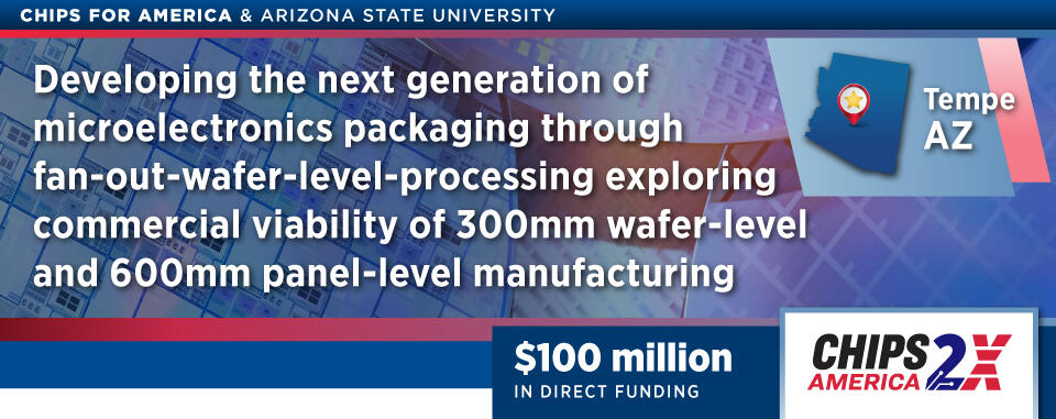
The U.S. Department of Commerce awarded Arizona State University (ASU) $100 million in direct funding to support the development of the next generation of microelectronics packaging through fan-out-wafer-level-processing (FOWLP). Centered at ASU Advanced Electronics and Photonics Core Facility, this project supports ASU’s research in exploring the commercial viability of 300 mm wafer-level and 600 mm panel-level manufacturing, a technology that does not exist as a commercial capability in the U.S. today.
Through ASU’s SHIELD USA (Substrate-based Heterogeneous Integration Enabling Leadership Demonstration for the USA) program, ASU, in close collaboration with Deca Technologies and numerous program partners, will design and develop molded core substrates that enable leap-ahead performance in organic substrate-based microelectronics packages.
Expected Outcomes
This award will help ASU develop molded core substrates with embedded components to support applications such as data center artificial intelligence (AI), edge AI, high-performance computing, advanced driver assistance systems, Internet of Things, and 5G/6G communications.
ASU will also extend fan-out wafer-level and panel-level packaging (FOWLP & FOPLP) technology by developing ultra-high-density planarized wiring, adaptive defect mitigation using maskless lithography to improve yield, novel vertical interconnect blocks for high-density through-core vias, new domestically produced build-up films, innovative embedded components, chip-design-like EDA tooling, design for test, fault tolerance techniques, and comprehensive modeling workflows to support design accuracy and reliability.
Advanced substrates funded by this award will be available for further process development within U.S. industry and other NAPMP programs. Additionally, this project will enable accelerated innovation in the advanced packaging ecosystem by providing access to proven process demonstration testbed.
Workforce Development
To support and expand the U.S. semiconductor workforce:
ASU will provide learning experiences and advanced packaging training programs for future generations of engineers and technicians.
ASU will develop training courses and microcredentials and will implement internship, apprenticeship, and researcher in residence programs for hands-on learning.
ASU will train and reskill current working professionals and raise awareness of microelectronics in K-12 students to expand the STEM pipeline to meet the domestic advanced packaging workforce demand for years to come.
About the CHIPS National Advanced Packaging Manufacturing Program (NAPMP)
To enable the CHIPS Research and Development Office’s vision for success, the CHIPS NAPMP will make approximately $3 billion in investments to develop critical and relevant innovations for advanced packaging technologies and accelerate their scaled transition to U.S. manufacturing entities. These investments will include research programs for core technologies that can be scaled to high-volume manufacturing, an advanced packaging piloting facility to support this scaling, resources to support the expansion of advanced packaging solutions, and workforce development. As a result, within a decade, NAPMP-funded activities, coupled with CHIPS manufacturing incentives, will establish a vibrant, self-sustaining, high-volume, domestic, advanced packaging industry where advanced-node chips manufactured in the United States are packaged in the United States. The technology developed will be leveraged in new applications and market sectors and at scale.
Financial Summary | Program | CHIPS NAPMP |
Direct Funding Amount | $100 million | |
Expected Co-Investment | $30 million |
Read the full CHIPS for America press release by clicking here.
Learn more about the CHIPS NAPMP by clicking here.