
Official websites use .gov
A .gov website belongs to an official government organization in the United States.
Secure .gov websites use HTTPS
A lock (
) or https:// means you’ve safely connected to the .gov website. Share sensitive information only on official, secure websites.
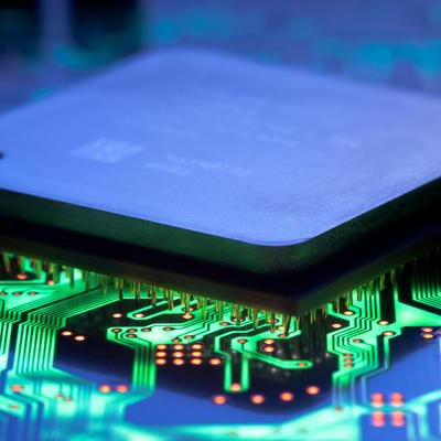
Semiconductors
The Material Measurement Science Division has a long history of working with stakeholders in the semiconductor industry to develop new measurement techniques and reference materials to meet their ever-changing metrology needs. Within our division, projects in this space fall generally into one of three categories: (1) 3D chemical and structural imaging, (2) nanomechanical property measurement, or (3) thermal property measurement. Additionally, our partnership with Brookhaven National Laboratory offers access to a unique suite of synchrotron-based measurement capabilities that are well aligned with the needs of the semiconductor industry.
Capabilities
MMSD possesses a large, diverse set of measurement capabilities and technical expertise that enables the division to meet the needs of our stakeholders in the semiconductor industry. Components of microelectronic devices cover the entire size spectrum from the nano- to micro- to macro-scale, and the techniques used to characterize these devices must span this entire range as well. In MMSD they are complemented with a strong metrological foundation as well as versatile material modeling capabilities. These measurement techniques include various imaging and characterization techniques and material property measurements, as well as micro- and nano-fabrication capabilities. Broken down by program, the breadth of these capabilities is demonstrated below.
- 3D Chemical and Structural Imaging
- Electron Microscopy (SEM, (S)TEM, FIB, EDS, EELS, tomography)
- Atom Probe Tomography (LEAP 4000X Si/HR – Local Electrode Atom Probe)
- 3D Optical Microscopy/Profilometry
- X-Ray Reflectivity (XRR)
- Secondary Ion Mass Spectrometry (SIMS)
- X-Ray Photoelectron Spectroscopy (XPS)
- Atomic Force Microscopy (AFM)
- Nanomechanical Property Measurement
- Contact Resonance Atomic Force Microscopy (CR-AFM) / Intermittent contact resonance atomic force microscopy
- Laser Doppler Vibrometry (LDV)
- Nanoindentation
- Electron Microscopy (EBSD, TKD, 4D-STEM)
- Raman Microscopy
- Thermal Property Measurement
- Nanocalorimetry Measurements
- Frequency Domain Thermoreflectance (FDTR)
- Differential Scanning Calorimetry (DSC)
- Dynamic Mechanical Analysis (DMA)
- Thermo-Gravimetric Analysis (TGA)
- Beamline Measurements (Brookhaven)
Supporting CHIPS for America
- Strain Measurement for Semiconductor Devices and Packages — Mechanical strain impacts the performance of semiconductor devices. Manufacturing processes must be carefully controlled for strain to achieve high-yield and high-performance products. However, measuring strain in nanoscale devices remains a metrology challenge for manufacturers. This project will advance techniques to measure strain, advance techniques, improve accuracy, and supply new reference materials to ensure capabilities for future-generation devices.
- Thermoreflectance Thermal Property Measurements for Heterogeneously Integrated Materials and Power Electronics — The thermal properties of materials and interfaces that govern the performance, reliability, and thermal management in microelectronics packages and wide bandgap power electronics are not fully or easily characterized, especially at device length scales wherein the properties can differ significantly from bulk or literature values. Transient Thermoreflectance (TR) is the emergent metrology that can characterize the thermal properties of films, multilayer structures, and their interfaces. This project will validate and improve emergent TR methods to provide data, protocols, and reference standards, leveraging our existing expertise and collaborations with instrument vendors and the semiconductor industry.
- Nanocalorimetry for Semiconductors and Semiconductor Process Metrology — Advanced methods to measure the thermal properties of thin films and interfaces are required to understand and improve microelectronic device fabrication, performance, heat dissipation and reliability. This project will build upon nanocalorimeters designed, fabricated, and calibrated at NIST to directly measure transition temperatures, reaction temperatures and specific heat capacity of nanoscale materials and devices for microelectronics, and support other efforts within the CHIPS R&D community.
- Non-Destructive Semiconductor Structure Function and Process Optimization for future Microelectronics Manufacturing at the NIST NSLS-II Beamline for XAFS and Diffraction — NIST Synchrotron beamline characterization of advanced semiconductor materials structure, chemical, electronic, and strain properties has been an ongoing pioneering metrology success for decades. This project will provide equipment enhancements to the existing NIST Synchrotron beamline for X-ray diffraction (XRD), and X-ray absorption spectroscopy (XAS) that will substantially increase sample throughput and sensitivity.
- Electron-Solid Interactions — Fundamental understanding of electron-solid interactions is key to interpreting electron microscopy images for quantitative metrology. Scanning electron microscopy (SEM) is a workhorse in microelectronics manufacturing and development. SEM is used for critical dimension, contour, and roughness metrology and for defect and failure analysis. However, the limitations of today’s physical models for electron-solid interactions directly affect microscopy measurement accuracy. This project will develop innovative models and data to validate and guide microscopy measurement accuracy.
- Characterization of Nano-to-Microscale Process-Induced Thermo-Mechanical Changes in Heterogeneously Integrated Microelectronics — Some of the manufacturing difficulties encountered by the heterogeneous integration of modular chips in system-in-package are due to thermal management and mechanical incompatibilities among the various interfaces and building blocks of the package. This project will provide indentation and scanning probe-based measurements of the thermo-mechanical properties of materials and structures used in advanced packages.
- Advanced Analytical Electron Tomography for Materials Development and Failure Analysis in Semiconductor Devices — Transmission electron microscopy (TEM) and scanning transmission electron microscopy (STEM) are widely used in industry for identifying structural and morphological characteristics in process development, control, and failure analysis. Existing TEM and STEM imaging methods struggle with complex semiconductor device architectures. This project will develop quantitative, atomic-resolution methods for the three-dimensional characterization of complex semiconductor devices via electron tomography.
- Multiscale Modeling and Validation of Semiconductor Materials and Devices — A comprehensive understanding of how current and next-generation materials impact the performance of semiconductor devices is critical to U.S. Semiconductor Manufacturing. This project will develop qualitative and quantitative models for advanced semiconductor heterostructures, including material properties and the impact of the interface quality via multi-scale, multi-fidelity computational approaches.
- Accurate Cure Kinetics, Stress, Mechanical Properties and Warpage — Advanced packaging involves increasingly challenging requirements for heterogeneous integration and chiplet packaging. Needs such as fine pitch interconnects (<10 μm pitch), finer lines/spaces, and an increasing number of distribution layers will require intensive engineering design to minimize warpage and maximize thermal performance while retaining or improving reliability in harsh conditions over the long-term life of the package. To be successful, research advances must address the most challenging materials and interfaces in the package, such as underfill materials, organic substrates, and molding and potting epoxies. Accurate material property measurements as a function of processing conditions, such as cure time, temperature, and pressure, are critical to inform the predictive models used to analyze how process tool requirements affect the warpage of integrated assemblies and packages. These critical properties must also be known as function of the harsh thermal and environmental conditions that chip packages are exposed to during their service. The outputs of this project include quantitative measurement methods, open-source materials data, model calibration frameworks, and predictive modeling tools to inform engineering design of advanced packaging systems in practice. These will be socialized with the semiconductor industry to drive polymer materials design and package design improvements required for 3D heterogeneous integration and to maintain standards modernity.
3D Chemical and Structural Imaging
Imaging techniques capable of measuring or mapping 3-D structures have widespread uses in the semiconductor industry. This includes dimensional metrology, chemical mapping, tomographic imaging, and countless others. In MMSD, there are many ongoing efforts targeted at advancing these techniques through the development of standards, reference materials, improved data collection techniques, and advanced analysis algorithms. A few specific efforts worth highlighting are:
- STEM Tomography — The architectural complexity of state-of-the-art and next-generation semiconductor devices makes failure analysis and process characterization difficult if not impossible. Performance and reliability can depend on single-atom defects and control of material structures and interfaces at levels that are not reliably measured by existing methods. A three-dimensional method of imaging the atomic- or near-atomic-scale structural and compositional features in such devices is of paramount importance for materials development and process control. Electron tomography is currently useful for semi-quantitative measurements of this kind at the nanometer length scale, however, it is plagued by reconstruction artifacts which limit its utility for critical-dimension evaluation, failure analysis, and other applications. MMSD researchers are actively collaborating with key industry stakeholders such as Intel and The Aerospace Corporation to develop quantitative 3D nano- and atomic-scale structural and chemical characterization methods based on electron tomography. The goal of this work is to produce quantifiable, high-fidelity 3D images of complex devices at the ultimate spatial resolution. By utilizing advanced specimen preparation protocols, automated data collection and analysis methods, along with advanced reconstruction algorithms, this work will address a critical industrial need.
- Dopant Quantification using Atom Probe Tomography — To ensure devices function properly, semiconductor manufacturers need to be able to control dopant concentrations at device dimensions with a high degree of accuracy. Atom probe tomography (APT) is uniquely capable of making these atomic-scale compositional measurements, however in some cases it can suffer from compositional measurement bias. To correct for this bias, MMSD scientists are investigating the value of a standards-based analysis approach, similar to what is commonplace for other analytical techniques. Using phosphorous-doped silicon as a test case, a NIST standard reference material (SRM 2133—P implant in Si depth profile standard) was analyzed under a variety of acquisition conditions. From this data, a calibration curve was generated by comparing the phosphorous concentration measured at each set of conditions to the known concentration from the SRM certificate. This calibration was then applied to a second, well-characterized silicon sample with a known phosphorous concentration. The uncorrected measurement was ~25% too low, however after applying the appropriate correction based on the calibration curve, this error was reduced to less than 4%. This same approach is currently being expanded to include other dopant types. In addition, to facilitate and accelerate adoption of this analysis method, a suite of new research grade test materials (RGTMs) is under development that are tailor-made for APT and span a wide range of industrially relevant materials for semiconductor applications.
Nanomechanical Property Measurements
We usually don’t think of semiconductor devices as mechanical systems, but even the most basic mechanical properties can have a large impact on device performance and reliability. Furthermore, devices are comprised of a wide variety of materials with dimensions spanning many orders of magnitude, each of which was chosen to perform a specific function in the device. The properties of these materials must be consistent from device to device and wafer to wafer, making any metrology techniques capable of identifying variations from expected behavior extremely valuable to the industry. MMSD has a wealth of expertise in this area to go along with existing collaborations with semiconductor manufacturers. A couple of efforts worth highlighting in this space include:
- CR-AFM — The continuous advances in semiconductor device fabrication demand various characterization techniques capable of proving accurate quantitative measurements at the nanoscale. A prominent scanning probe-based technique for nanoscale elastic property measurements is contact resonance atomic force microscopy (CR-AFM). In the past several years, we have continuously developed, improved, and expanded the CR-AFM technique with direct applications on surface and subsurface mechanical characterizations of the materials and structures used in Cu/low-k dielectric integrated circuits. Recently, we developed a quantitative methodology to test the elastic modulus and depth sensitivity of CR-AFM against a set of low-k dielectric bilayer films from Intel Corporation. The measurement analysis was accomplished by a combination of a semi-analytical and three-dimensional finite element analysis and provided a robust quantitative estimation of the subsurface depth and material sensitivities of CR-AFM. In this context, we developed a correlative measurement-model analysis to assess the convoluted contributions of the structural morphology and mechanical properties to the contact stiffness used by AFM-based subsurface imaging. The results explain the inherent difficulties associated with solving concurrently the material contrast and location of subsurface heterogeneities in nanomechanical subsurface imaging. Overall, these latest developments assert the capabilities of CR-AFM as a nondestructive and robust technique for probing layer thickness, subsurface features, and elastic properties of materials used in semiconductor electronics, additive manufacturing, or biomaterials.
- Strain Calibration Standard — Mechanical strain is very important to semiconductor devices and packages while also being difficult to measure accurately. Strain is engineered into CMOS channels to improve carrier mobility for higher performance at lower power but is also intrinsically present from manufacturing processes where strain can cause deleterious behavior and even failure through cracking and debonding. Device manufactures require metrology solutions for strain with front-end-of-line (FEOL) resolution (sub 10 nm) and strain accuracy better than 0.0005 m/m in Si to develop new devices, but the need for in-line or near-line strain measurements for fab process control are the major drivers of this project. Coincidently, quantum devices also have engineered and intrinsic strains (albeit for different reasons) that require development of essentially the same strain measurements. To address this need, NIST has developed a pair of reference materials (RM 8191/8192) consisting of strained Si1Ge1-x films on silicon substrates that can be used to calibrate existing measurement protocols, or benchmark new ones against. These products are in the final stages of certification and should be available by the end of 2023.
- NIST SRM 3461 Standard Reference Cantilevers — Atomic Force Microscopes (AFMs) are widely used in semiconductor metrology and can make a variety of useful measurements at very small scales. Many of these measurements, including those that probe mechanical and electrical properties, rely on accurate knowledge of the forces applied to the AFM tip when in contact with the sample surface. To that end, MMSD scientists developed, and recently released, SRM 3461, “Standard Reference Cantilevers for Atomic Force Microscopy Spring Constant Calibration.” This new NIST nanomechanical standard device comprises an array of seven well-characterized cantilevers that can be used to calibrate user’s own systems with significantly lower uncertainty (<3%) than via traditional methods (10% - 30%). This SRM was fabricated primarily in-house at the CNST NanoFab, and the stiffness of each individual cantilever on every chip was calibrated using Laser Doppler Vibrometry (LDV). SI-traceability was ensured by making comparative measurements using the NIST electrostatic force balance (EFB) in collaboration with PML.
Thermal Property Measurements
Thermal management is one of the most important and complicated problems involved in semiconductor device design. Doing so effectively not only requires accurate thermal property values for the individual materials involved, but the numerous interfaces between them as well. This is especially true in the advanced packaging community, where complexity and metrology needs are expanding rapidly. MMSD has several ongoing efforts in this space that are of interest to our stakeholders in the semiconductor industry, a few of which are highlighted below:
- Cure Kinetics of Packaging Materials — The cure kinetics of epoxy molding compounds (EMCs) are a critical material property that affects the reliability and performance of over-molded semiconductor chips. Accurate modeling of this material behavior is essential for accelerating R&D efforts in advanced packaging, where new technologies are being developed at an incredibly rapid pace. However, due to measurement challenges of today’s multi-resin EMCs, the semiconductor industry faces a challenge to perform accurate measurements, and often relies on over-simplified data analysis methods. The result is a potentially inaccurate prediction of residual stresses developed during manufacturing processes that may reduce reliability of the final package. To address this need, MMSD staff are developing measurement techniques capable of providing a more complete assessment of these materials and applying them to industry-standard products from a variety of leading vendors. With these techniques and materials data, stakeholders in the semiconductor industry will be able to develop more accurate models, as well as better optimization of manufacturing processes, than ever before.
- Nanocalorimetry Measurements — Nanocalorimetry is a nanoscale thermal measurement technique ideally suited to measure the thermal behavior of materials at fast rates and small dimensions, enabling quantification of previously inaccessible interfacial and thin film chemistry and physics. This makes the technique extremely useful for measurements of semiconductor materials, where complex thermal cycling often occurs across very small dimensions in multiple critical areas of devices. Ongoing efforts in this application space include collaborations with several academic, government, and industrial stakeholders to explore the behavior of candidate materials for new devices, such as phase change materials and thin-film phosphorus-rich CuP2, Additionally, this project is investigating how to integrate nanocalorimeters into semiconductor characterization and manufacturing tools for in-situ thermal measurements and process monitoring, with the goal being to provide real-time information to process engineers about process stability and any potential yield issues. And finally, thermal management with respect to advanced packaging and power electronics requires accurate knowledge of thermal material properties. Nanocalorimetry is well-suited for making these measurements for thin film and other nanoscale material systems, and efforts are currently ongoing to reduce the uncertainty of these measurements.
- Transport Property Measurements for Semiconductors and Energy Materials — The Transport Property Measurements for Semiconductors and Energy Materials project develops critical thermal and electrical transport measurement methods, instrumentation, and reference materials needed to support the development, performance, and reliability of bulk and thin film materials used in semiconductor microelectronics and energy conversion applications. A custom-built instrument for measuring electrical resistivity and Seebeck coefficient has been used to develop and publish best practice protocols and was essential in certifying SRM 3452, “High-Temperature Seebeck Coefficient Standard (295 K to 900 K)”. The Seebeck coefficient is a widely measured semiconductor property that provides fundamental information on charge carrier transport and the electronic structure of materials. A high-throughput version of this instrument has been used in conjunction with composition-spread film deposition to quickly and effectively screen ≈32,000 unique thermoelectric chemistries as part of collaboration with DOE, and to measure both additively manufactured and flexible inkjet-printed material libraries. Finally, in late 2022, the development of a new Frequency Domain Thermal Reflectance (FDTR) instrument was completed. This instrument is capable of measuring thermal conductivity, heat capacity, and thermal interface resistance of multilayered materials and thin films and will provide much needed property data to semiconductor manufacturers for effective design, modeling, and ultimately improvement of thermal management for microprocessors and wide bandgap semiconductor devices used for energy conversion applications.