
Official websites use .gov
A .gov website belongs to an official government organization in the United States.
Secure .gov websites use HTTPS
A lock (
) or https:// means you’ve safely connected to the .gov website. Share sensitive information only on official, secure websites.
Summary
Mechanical strain impacts the performance of semiconductor devices. Manufacturing processes must be carefully controlled for strain to achieve high-yield and high-performance products. However, measuring strain in nanoscale devices remains a metrology challenge for manufacturers.
This project will advance techniques to measure strain, advance techniques, improve accuracy, and supply new reference materials to ensure capabilities for future-generation devices.
Grand Challenge 2. Advanced Metrology for Future Microelectronics Manufacturing
Description
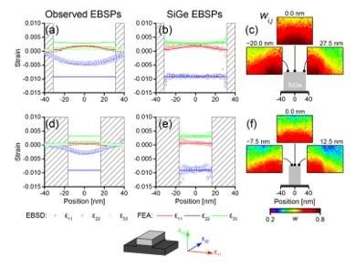
This image depicts an advanced analysis of HR-EBSD data to correct for the 3-D geometry of a strained nanoscale feature (in this case the fin of a FinFET). (a,d) show a clear mismatch between the original experimentally measured strains (data points) compared to the expected strains from FEA for features of different sizes. By applying the weighted correction factors depicted in (c) and (f) to those results, we are able to accurately capture the strain state and magnitude in the feature, regardless of size (b,e).
Strain is a critical parameter that influences both electrical and mechanical failures of devices, however, measuring strain in complex 3D geometries and vanishingly small feature sizes remains a challenge for manufacturers.
Data provided by strain measurements can be used to validate computational models of devices as well as simulations of manufacturing processes. Additionally, strain measurement is increasingly important in advanced packaging techniques, where vertical integration of components consisting of a wide variety of materials, using an equally wide variety of connection strategies, result in undesirable strains being introduced during fabrication and use. This reduces yield and causes failures while in service.
Improving the accuracy and uncertainty of these measurements, as well as developing strategies for employing them as close to the manufacturing line as possible will accelerate cycles of learning and deliver high yielding processes faster.
Industry needs robust strain measurement methods targeting fast in-line measurements for production and information rich near-/off-line techniques for R&D.
This is an ongoing project that has delivered industrially relevant solutions for over 10 years and continues to evolve to measure new structures with new methods to meet the needs of semiconductor manufacturing and R&D activities.
This project benefits industry by demonstrating strain measurements at a lab scale using new analysis approaches and equipment classes, as well as assisting to transition these measurements (or their calibrated surrogates) from lab to nearline, and nearline to inline metrologies. The lab scale outputs allow industry to reduce time and cost for cycles of learning on new process developments by enabling previously unavailable measurements of material properties. This allows shorter process development loops without completing fabrication and performing functional tests each cycle.