
Official websites use .gov
A .gov website belongs to an official government organization in the United States.
Secure .gov websites use HTTPS
A lock (
) or https:// means you’ve safely connected to the .gov website. Share sensitive information only on official, secure websites.
Non-Destructive Semiconductor Structure Function and Process Optimization for future Microelectronics Manufacturing at the NIST NSLS-II Beamline for XAFS and Diffraction
Summary
NIST Synchrotron beamline characterization of advanced semiconductor materials structure, chemical, electronic, and strain properties has been an ongoing pioneering metrology success for decades.
This project will provide equipment enhancements to the existing NIST Synchrotron beamline for X-ray diffraction (XRD), and X-ray absorption spectroscopy (XAS) that will substantially increase sample throughput and sensitivity.
Grand Challenge 2. Advanced Metrology for Future Microelectronics Manufacturing
Description
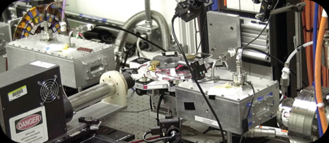
NIST’s Beamline for Materials Measurement (BMM) offers high-throughput, high-sensitivity X-ray Absorption Spectroscopy (XAS) tailored to studies of thin films and stacked structures. Systems studied by XAS include high dielectric materials for metal-insulator-metal stacks, oxidation and crystallization of deeply buried layers in MRAM stacks, and materials for quantum electronics.
This project relies on the existing NIST Synchrotron beamline for X-ray diffraction (XRD), and X-ray absorption spectroscopy (XAS) to improve measurement capabilities. The proposed equipment enhancements will substantially increase sample throughput and sensitivity. Driving the ability to probe deeper semiconductor device interfaces, a broader set of element/matrix combinations, and nanoscale probes of device stacks. These enhanced capabilities over the course of the next three years will be broadly available to the U.S. semiconductor industry through allocated beam time at the NIST beamlines. This broad and rapid accessibility of the new x-ray beamline metrology will directly enhance innovation and competitiveness in the U.S. semiconductor industry.
Making enhanced equipment for increased semiconductor testing and evaluation capabilities available to the broader CHIPS R&D community
This project will provide broad accessibility to the improved high throughput x-ray beamline metrology and will directly enhance innovation and competitiveness in the U.S. semiconductor industry for non-destructive semiconductor structure function and process optimization for future microelectronics manufacturing.