
Official websites use .gov
A .gov website belongs to an official government organization in the United States.
Secure .gov websites use HTTPS
A lock (
) or https:// means you’ve safely connected to the .gov website. Share sensitive information only on official, secure websites.
Joseph Woicik (Fed)
Research Interests
- High energy x-ray photoelectron spectroscopy: Applications to semiconductor gate stacks and Moore's law scaling. Direct measurements of the chemistry and bonding at semiconductor interfaces. Variable kinetic energy x-ray photoelectron spectroscopy for chemical depth profiling of electronic materials and interfaces.
- X-ray scattering: Applications to the hetero-epitaxial growth of semiconductor thin films. Diffraction studies of strain dependent structural and electronic phase transitions in transition-metal oxides. Diffuse x-ray scattering of defect structures in thin films.
- X-ray absorption fine structure spectroscopy of electronic materials: Local structure determination of dopant incorporation in implanted films, strain enhanced phase transitions in electronic materials, semiconductor gate stacks, and semiconductor diffusion barriers.
Postdoctoral Research Opportunities
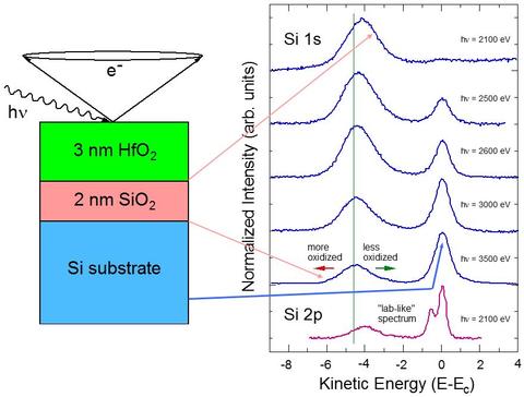
We have developed synchrotron based variable kinetic energy x-ray photoelectron spectroscopy to address the development and optimization of materials for microelectronics, catalysis, homeland security, and energy. Materials that can be investigated include monolayers to bulk materials of all classes. Depth selectivity is attained by utilizing different photon energies and core lines over a wide energy range. Examples of ongoing measurements include (1) chemistry and bonding at semiconductor oxide interfaces, (2) oxidation of metal electrodes on semiconductors, (3) ferroelectric oxides, (4) high-k gate dielectrics; and (5) organic electronics. Such measurement studies offer the opportunity to develop and utilize world class x-ray instrumentation and detectors. Similar materials are also characterized by x-ray diffraction and x-ray absorption fine structure spectroscopy to determine both their local and long range atomic structure in addition to the chemical information obtained from x-ray photoelectron spectroscopy.
Awards and Honors
- Department of Commerce Silver Medal Award, 2010
- Bronze Medal Award, U.S. Dept. of Commerce, 1998
- General Electric Fellow, Stanford University, 1983-1989