
Official websites use .gov
A .gov website belongs to an official government organization in the United States.
Secure .gov websites use HTTPS
A lock (
) or https:// means you’ve safely connected to the .gov website. Share sensitive information only on official, secure websites.
Summary
Fundamental understanding of electron-solid interactions is key to interpreting electron microscopy images for quantitative metrology. Scanning electron microscopy (SEM) is a workhorse in microelectronics manufacturing and development. SEM is used for critical dimension, contour, and roughness metrology and for defect and failure analysis. However, the limitations of today’s physical models for electron-solid interactions directly affect microscopy measurement accuracy.
This project will develop innovative models and data to validate and guide microscopy measurement accuracy.
Grand Challenge 2. Advanced Metrology for Future Microelectronics Manufacturing
Description
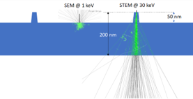
Measurement Intercomparison: More complex sample shapes will be fabricated on thin Si membranes in NIST’s NanoFab. The same features will be measured in secondary electron mode at low beam energy and in transmitted electron mode at high beam energy. The inferred shapes and dimensions should agree—if the models are correct. These data will encourage model development.
A measuring instrument produces a signal that depends upon the value of the measurand. The value and its uncertainty are inferred from the signal by using a model of their relationship. Erroneous models lead to erroneous inference. The accuracy of SEM (scanning electron microscopy) is limited by uncertainties associated with our incomplete knowledge of electron-solid interactions. The usual SEM imaging mechanism is secondary electron contrast.
Simulations that can accurately answer “what if” questions are important for design of new metrology techniques.
The variability of secondary electron yield measurements makes it challenging to use these measurements to qualify models. This project seeks to overcome those challenges. In addition to better understanding of secondary electron generation and transport, good simulations of backscattered electron yields from higher energy beams are needed because new technologies like gate all-around (GAA) transistors have working parts and associated defects that are buried too deeply to exhibit contrast in the lower energy secondary electron signal.
Insulators are used to isolate circuit elements from each other. This means there is need for SEM images of regions that contain insulators and consequent demand for models that can account for charging.
The project will concentrate on SEM metrology, however, the improved electron-solid interaction models and validation data developed will have synergistic applications to other electron-beam techniques and spectroscopies.