U.S. flag

An official website of the United States government

Official websites use .gov
A .gov website belongs to an official government organization in the United States.

Secure .gov websites use HTTPS
A lock ( ) or https:// means you’ve safely connected to the .gov website. Share sensitive information only on official, secure websites.

Projects/Programs

Displaying 76 - 100 of 112

Nanophononic Metamaterials for Thermoelectrics

Ongoing
About 68 % of the energy produced in the United States is wasted as heat lost to the environment. About a quarter of this lost heat is present at temperature gradients suitable for recovery with thermoelectric devices, which use the ability of semiconductors to generate electricity directly from...

Nanoscale, Element-Specific X-ray Imaging for Integrated Circuit Metrology

Ongoing
Industry roadmaps identify the characterization of nanoscale subsurface feature shape and composition as a measurement need for the semiconductor industry. However, IC interiors are difficult to probe post-manufacturing due to the presence of many close-packed and nanoscale subsurface features, of...

Nanoscale Property Measurements by Atomic Force Microscopy

Ongoing
Over the past several decades, Atomic Force Microscopy (AFM) has advanced from a technique used primarily for surface topography imaging to one capable of characterizing a range of chemical, mechanical, electrical, and magnetic material properties with nanometer resolution. Such characterizations...

Nanostructure Fabrication and Metrology

Completed
This project develops semiconductor nanostructures, especially self-assembled quantum dots and photonic crystals, for a variety of applications including single photonics, laser diodes, and quantum optical metrology. It also develops quantum optical metrology based on other sources and detectors...

The Nanotechnology Xccelerator

Ongoing
The Nanotechnology Xccelerator was announced on September 13, 2022 and was officially accepted for production at Skywater Technology Foundry using the Sky130 technology in Q1 2024. Sky130, which comes in both a conventional and open-source process design kit, is a 5-metal layer process. To...

Neuromorphic Device Measurements

Ongoing
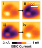
One type of device that is emerging as an attractive artificial synapse is the resistive switch, or memristor. These devices, which usually consist of a thin layer of oxide between two electrodes, have conductivity that depends on their history of applied voltage, and thus have highly nonlinear...

Novel Sources for Focused-ion Beams

Completed
Commercial focused ion beams (FIBs) are used in a wide variety of applications. For example, they serve as diagnostic tools, slicing through a nanodevice to expose its internal structure. They can also shape nanoscale materials either by adding atoms to a structure or by shaving them off. And they...

Optical and Microwave Spectroscopy of Microelectronic Systems

Ongoing
Collaborations with industry leaders have led to new understanding of magnetic damping in advanced materials and replication of our magnetic metrology tools. We investigate fundamental aspects of spin transfer in materials and structures that offer improved performance in future devices such as...

Optical Probes of 2D Magnetic Phenomena

Ongoing
The unique measurement capabilities developed in this Project enable diffraction-limited, optical spectra (both Raman and photoluminescence) to be collected and analyzed as a function of laser energy, polarization, temperature, magnetic field, and device parameters such as current load and back...

Plasma Process Metrology

Ongoing
Intended Impact The model for rf bias effects that we have developed should make it easier for industry to select optimal operating frequencies and may stimulate the adoption of new methods for RF biasing, such as multiple-frequency bias and non-sinusoidal bias. NIST studies of electrical endpoint...

Polymers for Next-Generation Lithography

Completed
We work closely with the semiconductor industry to develop and apply measurements with high-spatial and chemically-specific resolution to elucidate the critical materials properties and process kinetics at nanometer scales that are needed to advance next-generation photolithography, including both...

Power Conditioning Systems for Renewables, Storage, and Microgrids

Completed
Objective: To establish standards and measurement methods, and test for smart grid and microgrid Power Conditioning Systems needed to transition from today’s low penetration of nondispatchable intermittent renewable energy sources to flexible grid operations that can actively adjust to varying grid...

Precision Materials for Quantum Devices

Ongoing
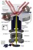
MBE System Our fabrication system is composed of ultra-high vacuum (UHV) chambers that support the in-vacuum exchange of 75 mm wafers without exposure to air as seen in Figure 1. These chambers are: (1) a deposition chamber with electron gun deposition, UHV compatible sputter guns, in situ shadow...

Prototyping Platforms for Emerging Technologies

Ongoing
Emerging technologies aim to overcome traditional memory limitations with higher density, lower power consumption, faster read/write speeds, better endurance, and lower cost [2]. Many new candidate memory elements are analog or stochastic, requiring new testing infrastructure, and the context of...

Pushing the Limits of Measurement Accuracy in Atom Probe Mass Spectrometry

Ongoing
Isotopic Analysis for Isotopic Geochemistry, Nuclear Safety, and Materials Science : Atom probe tomography has a significant advantage over other forms of mass spectrometry, which typically have a combined efficiency < 5%, in terms of ionization and detection efficiency. Commercial atom probe...

Reliability Metrologies for Advanced Electronic Interconnects

Completed
High-performance devices, such as microprocessors and memory chips, are typically composed of structures with strict dimensional tolerances and geometries and are made up of various materials, all in close proximity in a three-dimensional system. Material interactions lead to reliability issues such...

Semiconductor Nanowire Metrology: Electronics, Photonics, and Sensors

Completed
One of the key issues hampering progress in semiconductor nanotechnology is the absence of standardized nanostructures. We address this need through the controlled fabrication and assembly of semiconductor nanowire test structures with well-defined properties. To achieve this, we have manufactured...

Smart Grid System Testbed Facility

Completed
Objective: To develop an advanced multi-mode interacting measurement testbed to facilitate implementation, validation, and full characterization of smart grid interoperability standards and smart grid performance. What is the technical idea? An interacting multi-mode measurement and characterization...

Spectroscopy and Application of Solid-State Quantum Centers

Ongoing
Quantum color centers in wide-bandgap semiconductors have spin and optical degrees of freedom, which can be leveraged for applications such as sensing and single-photon generation. In materials like diamond and silicon carbide, long spin lifetimes and quantum coherence times enable sensitive...

Strain Measurement for Semiconductor Devices and Packages

Ongoing
Strain is a critical parameter that influences both electrical and mechanical failures of devices, however, measuring strain in complex 3D geometries and vanishingly small feature sizes remains a challenge for manufacturers. Data provided by strain measurements can be used to validate computational...

Strain Measurement for Semiconductor Devices

Ongoing
Mechanical strain is hugely important to semiconductor devices and packages while also being difficult to measure accurately. Strain is engineered into CMOS channels to improve carrier mobility for higher performance at lower power but is also intrinsically present from manufacturing processes where...

Sub-nanoscale electron microscopy of complex nanostructures

Ongoing
The properties of advance materials are becoming ever more reliant on the ability to manipulate their chemistry and structure at very fine length scales. For example, the relevant feature sizes in state-of-the-art transistors continue to decrease, even as the complexity of the architectures employed...
Was this page helpful?