
Official websites use .gov
A .gov website belongs to an official government organization in the United States.
Secure .gov websites use HTTPS
A lock (
) or https:// means you’ve safely connected to the .gov website. Share sensitive information only on official, secure websites.
Summary
The Nanotechnology Xccelerator is a pilot program to develop a powerful new family of foundry platforms and test vehicles for academics to do scientific research and workforce training in CMOS+X technologies and analog circuit design. The system is designed to be robust for use in research cleanrooms, compatible with common academic lithographic marks, planarized for integration, and features 30 unique projects common to the CMOS+X research space. The projects range from the integration of individual memory devices to array-level macros, bioelectronic test vehicles, and even cryogenic electronic test vehicles. The chips are combined into one flash field as a unique Multi-Project-Multi-Facility mask set.
Developing the platform required programmatic support from industrial partners like Google, Skywater, Western Digital, and Cadence Design Systems, as well as the individual contributions of 14 principal investigators in integrated circuit design.
With the Nanotechnology Xccelerator, it becomes possible to bring a wafer-scale platform from a fabrication facility into the academic nanofab and laboratory settings.
Description
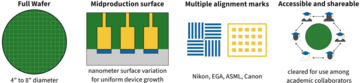
The Nanotechnology Xccelerator was announced on September 13, 2022 and was officially accepted for production at Skywater Technology Foundry using the Sky130 technology in Q1 2024. Sky130, which comes in both a conventional and open-source process design kit, is a 5-metal layer process. To facilitate integration into research fabrication facilities, the Nanotechnology Xccelerator only uses 4 of the 5 metal layers, and wafers are provided with tungsten vias exposed to the surface immediately after a chemical mechanical polishing step.
To facilitate introduction into research facilities, a special test chip has been developed which contains a large diversity of alignment marks. These include marks for ASML PAS steppers, Nikon steppers, Canon steppers, GCA steppers, contact lithography, and e-beam lithography. The marks are placed on the tile in quadruplicate. It’s possible to acquire the Nanotechnology Xccelerator in a 200 mm wafer scale form factor which can be used as-is, cored to 150 mm or 100 mm, or diced into coupons. Dicing through the alignment mark tile will allow marks to be placed on each of the four corners of the coupon while simultaneously leaving enough room for photoresist to spin.
The full wafer can be acquired as a multi-project-multi-facility test vehicle thanks to innovative licensing options provided by Google, Skywater, and Cadence Design Systems. While some of the dies take advantage of open source Apache licensing from the open source process design kit, others received assistance from Cadence’s granting of a license to academic researchers to share silicon with academic partners from designs derived using the Cadence Academic Network. This contribution has been necessary to ensuring the success of the program.
Core features that make it useable for a research nanofabrication facility.
This unique combination of features – wafer scale form factor, high quality surface, diverse alignment marks, and the appropriate legal permissions – makes the Nanotechnology Xccelerator an innovative new approach to providing university researchers with an accessible, usable platform for CMOS+X research.
Background
VLSI researchers historically have had good access to multi-project wafer (MPW) programs, allowing them to source chips for circuit design research. Such work requires constant access to newly developed commercial technologies and a steady stream of new topics in circuit design. In contrast, nanofabrication and nanodevice researchers have not had as good access to silicon substrates with pre-patterned test/measure capability for CMOS+X research. The reason for this is that nanofabrication research requires wafers instead of individual chips, special surface preparation lithographic compatibility, and appropriate licensing. The challenge for academic researchers to access foundry technology has been highlighted many times in a variety of workshops (see here and here and here) and national academy reports.
To overcome these issues, the Nanotechnology Xccelerator program was kicked off in 2022 at the NIST Integrated Circuits for Metrology Workshop, an event with over 300 attendees. The program was launched by NIST staff as an outgrowth of existing NIST programs in CMOS test vehicles and hardware-based artificial intelligence. Contributors volunteered their time to create a new family of test vehicles for CMOS+X technology, academic research, and workforce training. Starting in Spring 2023, NIST and contributors convened weekly technical development meetings to design the chips. During summer and fall, technical experts were brought in during periodic design review sessions to ensure that the various chips were appropriate for their intended purpose and could be integrated into nanofabrication facilities. The final reticle set was accepted by Skywater in Q1 2024 for production.
The program resulted in 30 contributed tiles for nanofabrication research to be fabricated in a Skywater 130 CMOS process. These tiles are geared toward pre-competitive CMOS+X research and semiconductor fabrication integration.
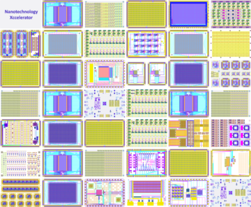
Layout of the Nanotechnology Xccelerator Reticle with 30 unique tiles occupying 41 different slots within the reticle.
Types of Projects
Projects fall primarily into 3 types: test structures for parametric test, array-level test macros, and bioelectronic test vehicles. The parametric test structures are as simple as single transistors and as complicated as isolated cryogenic operational amplifiers which can be directly co-integrated with novel nanodevices. Array-level test macros include chips designed for 2-terminal and 3-terminal back-end-of-line integrated memory or selector devices. However, they could be used for any array-level characterization of any compatible nanodevice. The bioelectronic test vehicles include diverse circuits such as ion-sensitive field-effect transistors, capacitive sensors, and picoampere-sensitive current amplifiers. These bioelectronic chips are primarily used for addressing unsolved problems in semiconductor manufacturing related to optimized semiconductor bioelectronic interfaces.
In addition to the three primary tile types, there is also one transistor array that has been developed as an analog gate array for integrated circuit design education. This unique array can be programmed using a single lithographic step with a conventional laser writer. This design can enable a university student to “tape-out” a six-thousand-transistor circuit in as few as 24 hours.
Individual Teams and Projects
Individual chips were designed by fourteen different principal investigators from ten different institutions. Nanofabrication engineers and researchers, including from industrial partners, helped during design reviews to ensure that the proposed projects could be accessible to users. A summary of the all the different project contributions can be accessed here.
Contact
Interested parties should contact us nanotechnologyxccelerator [at] nist.gov (here) via email.