Summary
Our goal is to develop measurement methods with sufficiently high spatial resolution to uncover the materials limitations in the resolution of state-of-the-art photoresist formulations. Photolithography, the process used to fabricate integrated circuits, has been the key enabler for performance advances in the microelectronics industry. However, as the lithographically patterned features decrease towards length scales of 32 nm, challenges arise because photoresists appear to be reaching their resolution limits. Our measurements help define these limits and enable the development of higher resolution photoresists and lithographic processes.
Description
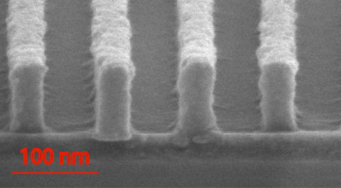
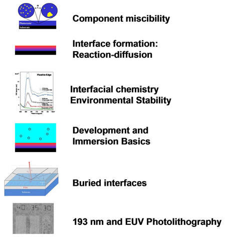
We work closely with the semiconductor industry to develop and apply measurements with high-spatial and chemically-specific resolution to elucidate the critical materials properties and process kinetics at nanometer scales that are needed to advance next-generation photolithography, including both the 193 nm (deep ultraviolet, DUV) and 13.5 nm (extreme ultraviolet, EUV) lithography platforms. This provides the foundation for the rational design of materials and processing strategies for the fabrication of sub-32 nm structures. Our innovative measurement platform integrates specular and off-specular X-ray and neutron reflectivity, near-edge X-ray absorption fine structure spectroscopy, quartz crystal microbalance, solid state nuclear magnetic resonance, polarization-modulation infrared reflectance absorption spectroscopy, and infrared variable angle spectroscopic ellipsometry. These measurements relate the fundamentals of polymer interfaces to high resolution lithographic patterning.
Major Accomplishments
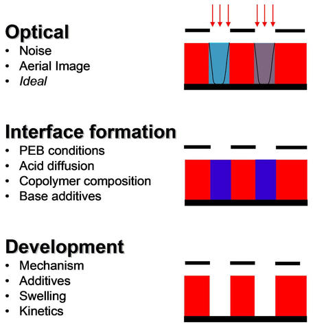
- With more that $43 Billion in exports in 2005, the semiconductor industry is the leading U.S. exporter and provides more than240,000 domestic jobs.
- NIST successfully completed a two-year contract with SEMATECH on quantifying the materials sources of line-edge roughness which causes excess chip power consumption and process speed variation.
- NIST developed and transferred FTIR based reaction-kinetics tools and modeling software to Intel.This method is being used by Intel to independently benchmark photoacid diffusion length for advanced photoresist formulations and optimize parameters for their manufacturing processes.
- World's first measurement of the buried in-plane reaction-diffusion profile and latent-image swelling by neutron reflectivity and diffuse scattering methods provided critical data on how resist processing contributes to line-edge roughness, a measure of ultimate resolution.
- CRADA with Intel to develop quartz-crystal microbalance methods to characterize photoresist swelling which impacts resolution of model and commercial photoresists.
Additional Technical Details
Latent Image Formation:
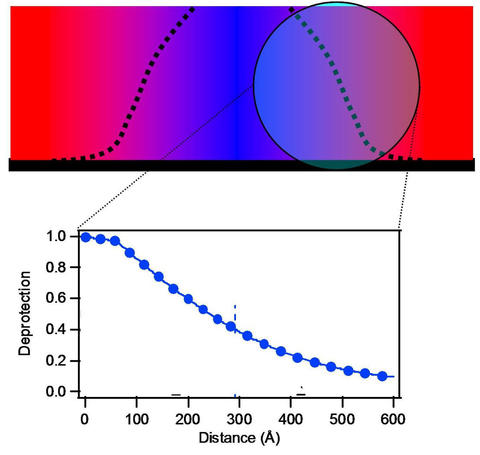
In current 193 nm dry, future immersion, and EUV photolithography, high resolution imaging is performed by converting an optical image into a chemical latent image within a photoresist. This chemical latent image is formed by the diffusion of photoacid catalysts which can limit the ultimate resolution characterized by feature size and undesirable line-edge roughness. Under ideal optical conditions produced by a model bilayer test structure, the deprotection reaction front profile was measured with nanometer resolution by combining neutron reflectivity and infrared spectroscopy on model 193 nm and EUV photoresists.The upper layer of the structure is loaded with the photoacid generator. Upon exposure and baking, the photoacid diffuses into the lower layer and catalyzes the deprotection reaction. These resulting reaction fronts are are the first available with nm spatial resolution. Among our results, we found that the reaction front width is strongly controlled by resist chemistry, exposure dose, PAG size, and amine quencher. These experimental data provide a rational design of next-generation photoresist component from the resist chemistry to the reaction-diffusion process.
Image Development:
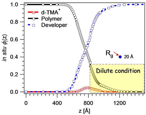
The chemical latent image determines the nanoscale regions of resist that are soluble in situ development profiles at line-edge in the aqueous base developer solution that produces the final pattern. As these feature dimensions approach sub-32 nm, however, a possible trade-off among process variables may limit photoresists from achieving less than 2 nm LER design criteria. A central assumption in these resolution limit models is a direct transfer of the chemical latent image heterogeneity on the feature quality. Insight into the mechanism of development, rinse, and drying at a gradient line edge was achieved by neutron reflectivity with nm resolution. Direct measurements of the highly swollen photoresist polymer, deuterium labeled developer (d-TMA+) and aqueous solvent profiles at the developed line-edge clearly highlights a residual swelling fraction with spatial dimensions that exceed the radius of gyration of the photoresist polymer. The final surface roughness is formed by the collapse of this highly associated phase during the drying process.A mechanism of a simple transfer of roughness from the latent image to the developed image is challenged by these data.
Metrology for Immersion Lithography:
Next-generation lithography will use an immersion fluid between the lens and photoresist.This leads to undesirable leaching of critical components that will cause undesirable defect formation.The change in component distribution, such as photoacid generators, within the top 8 nm at the surface of the thin film may be observed by examining the near-edge X-ray spectra of light elements such as carbon, oxygen, fluorine, and nitrogen.In this way, changes in the surface chemistry relative to the bulk film can be investigated as a function of lithographic processing steps. We have found that fluorinated PAG molecules preferentially segregate to the film surface.

The relative amount of segregation is dependent upon the specific polymer chemistry and PAG size (TPS-triflate< TPS-PFBS <TPS-PFOS). NEXAFS measurements quantify the influence of water immersion on the depth profile and loss of these critical components. When combined with liquid chromatography/mass spectrometry, the equilibrium water solubility of PAGs with varying perfluoroalkyl length does not serve as the appropriate criteria for selecting PAGs for immersion lithography; rather the segregation of PAGs to the top few nanometers provides the majority of leaching.

