
Official websites use .gov
A .gov website belongs to an official government organization in the United States.
Secure .gov websites use HTTPS
A lock (
) or https:// means you’ve safely connected to the .gov website. Share sensitive information only on official, secure websites.
Quantitative Assessment of Defects and Related Modeling Parameters in GaN Semiconductor Devices
Summary
The power electronics and radio frequency (RF) communications industries increasingly rely on semiconductors in the GaN/AlGaN family, where performance is limited by material defects. Being able to predict defect behavior is essential in device design, but the necessary data is often lacking.
This project will produce modeling data on a broad range of defects in GaN, AlGaN, and SiC, and identify the physical and chemical structure of these defects to assist foundries in eliminating them.
Grand Challenge 4: Modeling and Simulating Semiconductor Materials, Devices, and Components
Description
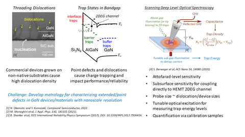
Key performance metrics like breakdown voltage, switching speed, gain stability, and maximum operating frequency are limited by material defects in AlGaN/GaN devices. Defects also play a role in device degradation over time. Although these materials have been studied for over twenty years with a variety of methods, including photoluminescence (PL), deep level transient spectroscopy (DLTS), deep level optical spectroscopy (DLOS), Transmission Electron Microscopy (TEM), and device electrical characterization, there are many types of defects, and they are poorly understood. Electrical signatures of defects are relatively easy to collect, but figuring out the physical and chemical structure of the defects is extremely challenging.
Controlling defects in these semiconductors will lead to rapid performance advancement for the electrification of the U. S. economy and 5G/6G communications, resulting in energy savings and climate change mitigation.
This project will develop multiple techniques to locate and characterize defects in GaN, AlGaN, and SiC. By using complementary methods that extract electrical, spectral, and structural properties, new insight into the physical origins and electrical behavior of defects can be achieved.
This data will be organized to allow incorporation into multi-physics models that predict noise performance, thermal properties, reliability, and energy efficiency. This project will also improve the tools needed to effectively model and simulate future semiconductor materials and devices by quantifying the characteristic properties of traps and defects that are present in commercial materials and quantify how they affect carrier transport properties.
The measurements made in this work will have immediate relevance to the semiconductor ecosystem.