
Official websites use .gov
A .gov website belongs to an official government organization in the United States.
Secure .gov websites use HTTPS
A lock (
) or https:// means you’ve safely connected to the .gov website. Share sensitive information only on official, secure websites.
Overcoming Barriers: Nanoscale Interface Metrology and Electrical Characterization for Advanced Electronics
Summary
As devices become smaller, more complex, and more highly integrated, interfaces are increasingly important and limiting. The ability to accurately predict interface behavior is critical for accelerating device development times but requires atomic-scale knowledge of interface electric fields, which is currently unavailable.
This project will develop standardized data collection and analysis protocols to enable nanoscale electric field determination from artifact free differential phase contrast four-dimensional scanning transmission electron microscopy (DPC 4D-STEM) data.
Grand Challenge 2. Advanced Metrology for Future Microelectronics Manufacturing
Description
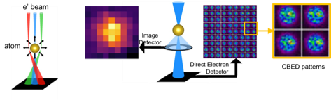
The STEM electron probe is deflected by the sample electric field. In 4D-STEM 2D diffraction patterns are collected at a 2D grid of positions, enabling atomic scale measurement of structure, composition, bonding, orientation, strain, and electric field.
“The interface is the device,” Herbert Kroemer, 2000 Nobel Laureate. This is even more true today, twenty-three years later, when device dimensions are measured in numbers of atoms rather than numbers of micrometers. Historically, interface problems in the semiconductor industry have been addressed empirically, but it is increasingly urgent to have reliable nanoscale measurements for device development, for failure analysis and for development of reality based predictive models.
The behavior of all electrical devices is controlled by band offsets, which directly control contact resistance, threshold voltage, leakage current and reliability. Managing the offset for each of these interfaces remains a challenge to be navigated with each new generation of advanced electronics.
The NIST published protocols and data analysis software for mapping electric field on the atomic scale will enable industry to obtain this information on interfaces of relevance today and in the future, promoting faster development times and fabrication optimization.
True understanding and control of interfaces requires atomic scale knowledge of interface structure, composition, bonding, strain, and electric field. While the small probe size and high current density of aberration corrected scanning transmission electron microscopes has enabled many of these measurements, determination of the electric field on the atomic scale remains problematic.
This project will develop DPC 4D-STEM techniques and data processing methods to make atomic scale measurements of the electric field more widely accessible. This will ensure the electronics industry has access to the information they need to design increasingly complex, ever shrinking devices. The data obtained during development of the technique will provide guidance on how to achieve interfaces with desired band offsets to meet future technology requirements.