Summary
Our objective is to develop metrology techniques for characterizing mechanical strain in semiconductor devices as well as reference materials for assessing the accuracy of those techniques.
Description
Mechanical strain is hugely important to semiconductor devices and packages while also being difficult to measure accurately. Strain is engineered into CMOS channels to improve carrier mobility for higher performance at lower power but is also intrinsically present from manufacturing processes where strain can cause deleterious behavior and even failure through cracking and debonding. Device manufactures require metrology solutions for strain with FEOL resolution (sub 10 nm) and strain accuracy better than 0.0005 m/m in Si to characterize the next generation of devices, but the need for in-line or near-line strain measurements for fab process control are the major driver of this project. Coincidently, quantum devices also have engineered and intrinsic strains (albeit for different reasons) that require development of essentially the same strain measurements.
We have collaborated with industry for over a decade on various aspects of strain metrology in semiconductor devices. We have applied commercial techniques to industry-provided samples, developed new measurement instruments and data analysis techniques, worked with vendors to improve the accuracy of the results from commercial systems, and manufactured strain reference materials to enable calibration and verification of measurement systems and techniques.
Major Accomplishments
Semiconductor Strain Calibration Artifact (RM 8191/8192)
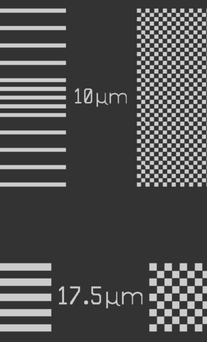
We have produced two reference materials intended for use as calibration artifacts for strain measurements, or to assess the accuracy of new measurement techniques. These RMs consist of a strained, epitaxial SixGe1-x film on a silicon substrate, and are available with two different SixGe1-x compositions, resulting in different tetragonal strain magnitudes. The films are patterned with a variety of feature types and sizes, allowing for relative measurements between the film and underlying substrate to be made by a variety of techniques. A large area of unpatterned film is also present to allow for x-ray diffraction measurements, which were used to certify the strain value for each individual chip.
Release date: TBD (Contact William Alexander Osborn for more details)

Strain Measurement of 3D Structured Nanodevices by HR-EBSD
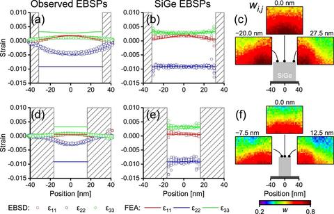
Accurate measurement of strain in sub-100nm SiGe-Si fin structures is important for both device development and manufacturing process control. HR-EBSD provides strain results for these structures, however, nanoscale 3D features present unique challenges for a technique developed primarily for planar samples. Executing typical HR-EBSD analysis on a nanoscale 3D fin yields incorrect strain magnitudes that vary with fin width. To address this issue, we developed a new analysis procedure to correct EBSD patterns that are convolved from the sample and substrate regions. This deconvolution is informed by electron trajectory simulations and yields EBSD patterns that can be analyzed using typical HR-EBSD analyses, and significantly improve the accuracy of the method for this class of samples.

Strain Measurement Surrounding Tungsten-filled Through Silicon Vias (TSVs)
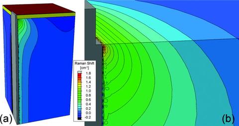
Microfabricated structures experience strains induced by unavoidable residual stresses resulting from the growth and deposition of materials. TSVs can impose large stresses and strains on the Si surrounding the via that must be accommodated in device design rules. Optimization of these design rules requires validated models of the strain field surrounding a TSV. Because the strain state near a TSV is not simple, we developed code to extend the capabilities of commercial finite element analysis tools so that Raman shift could be calculated as a field output. This allows direct comparison of confocal Raman microscopy data to simulations and provides essential feedback to validate modeling assumptions including geometry and material properties.


