
Official websites use .gov
A .gov website belongs to an official government organization in the United States.
Secure .gov websites use HTTPS
A lock (
) or https:// means you’ve safely connected to the .gov website. Share sensitive information only on official, secure websites.
Confocal Raman Microscopy: A Platform for Mapping Stress in Materials
Summary
Researchers in the Nanomechanical Properties Group, Materials Measurement Science Division, MML have applied high spatial resolution, confocal Raman and luminescence microscopy techniques to the characterization of the spatial variation of stress in semiconductor, ceramic and glass materials.

DEScription
Confocal Raman microscopy is a powerful tool for the characterization of materials on microscopic length scales. The specific patterns of scattering resonances measured in this vibrational spectroscopy reveal information about the chemical composition of specimens. In certain cases, analysis of band shifts, line shapes and polarization dependence can also provide insight into other material characteristics of interest, including stress, crystallinity and orientation. Specimens typically do not require extensive sample preparation and the attainable analysis volume is often limited only by diffraction. The instrumentation can also be readily adapted to the measurement of narrow band luminescence in materials.
The presence of stress in certain materials can result in shifts in the energy of characteristic spectral features, including Raman and luminescence bands. Stress induced perturbations in the atomic structure result in subtle variations in the lattice vibrational modes (Raman) or electronic structure (luminescence) compared to the unperturbed material. This phenomenon, widely referred to as the piezospectroscopic effect, can be exploited to measure stresses in materials in a non-contact manner at diffraction limited spatial resolutions. The NIST research team has applied this general approach to the study of externally applied stresses (e.g., nanoindentation) and stresses resulting from processing (e.g., residual thermal stress, micromachining) in several classes of materials, including semiconductors, ceramics and glasses.
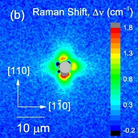
Stress mapping in silicon takes advantage of a variation with stress in the energy of the Raman band due to the LO (longitudinal optical) phonon at approximately 520.6 cm-1. The energy of this Raman band can be measured with high precision at every point in an image allowing the construction of a spatial map of the material stress. The NIST team has employed this technique in the mapping of stress in micromachined polysilicon features held in uniaxial tension. These measured stress magnitudes and spatial variations compared favorably with results predicted by finite element analysis. Raman stress mapping in these types of devices allow the identification of design defects that may limit device lifetimes and thus enable processing improvements to improve device reliability. Stress mapping has also been applied to the study of stress in and around line and spherical indentations in silicon as seen in the Figure 1. Stress images of these indentation features were also in quite good agreement with predictions made on the basis of electron backscatter diffraction data from the same indents.
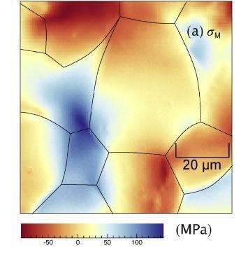
Stress mapping in alumina ceramics by luminescence microscopy takes advantage of two emission bands (R1 and R2) of Cr ion impurities in Al2O3 at approximately 694 nm. These bands originate from the crystal field established by octahedral coordination of O ions surrounding the Cr impurity ion. Stress, among other factors, results in a perturbation of the crystal field and a subsequent subtle shift in the energy of the R1 and R2 bands. The microscope is configured to record a luminescence spectrum of the R1 and R2 bands at each spatial position in the map; extracting the shifts leads directly to a stress map of the specimen. The NIST research team has used this approach to study the spatial variation in residual thermal stresses in and around single grains in sintered alumina as is shown in Figure 2. The same approach is also being used to study the variation in stress near the braze/ceramic interface in specimens with ceramic-metal joints in a collaboration with researchers from Sandia National Labs.
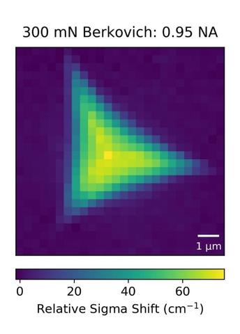
In anomalous glasses, the application of external mechanical stress results in densification. This material response is reflected in variation in the shape and position of the Raman bands of fused silica and other related glasses. Confocal Raman microscopy can be used to generate maps of a band shift parameter, sigma, that is related to the degree of glass densification. This approach can then be employed to study the effects of various factors, including composition, loading conditions and indenter geometry, on the glass deformation process. The sigma shift image of a residual indent created by a 300 mN indentation of fused silica with a Berkovich indenter is shown in Figure 3. Recent work has focused on understanding and establishing the experimental conditions under which the glass analysis volume is small relative to the deformation volume as is necessary for meaningful measurements.
MAJOR ACCOMPLISHMENTS
- R.F. Cook and C.A. Michaels, " Stress measurements in alumina by optical fluorescence: revisited," J. Res. Natl Inst. Stan., 124:20 (2019). https://doi.org/10.6028/jres.124.020
- C.A. Michaels and R.F. Cook, " Residual stress in polycrystalline alumina: Comparison of two-dimensional maps and integrated scans in fluorescence-based measurements," Acta Mat., 159 309 (2018). https://doi.org/10.1016/j.actamat.2018.08.025
- A.J. Gayle, L.H. Friedman, R. Beams, B.G. Bush, Y.B. Gerbig, C.A. Michaels, M.D. Vaudin, and R.F. Cook, "Two-dimensional strain-mapping by electron backscatter diffraction and confocal Raman spectroscopy," J. Appl. Phys., 122 205101 (2017). https://doi.org/10.1063/1.5001270
- R.F. Cook and C.A. Michaels, "Coefficients for stress, temperature, and composition effects in fluorescence measurements of alumina," J. Res. Natl Inst. Stan., 122:43 (2016). https://doi.org/10.6028/jres.122.043
- G.A. Myers, C.A. Michaels, and R.F. Cook, "Quantitative mapping of stress heterogeneity in polycrystalline alumina using hyperspectral fluorescence microscopy," Acta Mat., 106, 272 (2016). https://doi.org/10.1016/j.actamat.2016.01.020
- C.A. Michaels and R.F. Cook, "Determination of residual stress distributions in polycrystalline alumina using fluorescence microscopy," Mater. Design, 107, 478 (2016). https://doi.org/10.1016/j.matdes.2016.06.063
- G.A. Myers, S.S. Hazra, M.P. deBoer, C.A. Michaels, S.J. Stranick, R.P. Koseski, R.F. Cook, and F.W. DelRio, "Stress mapping of micromachined polycrystalline silicon devices via confocal Raman microscopy," Appl. Phys. Lett., 104, 191908 (2014). https://doi.org/10.1063/1.4878616