
Official websites use .gov
A .gov website belongs to an official government organization in the United States.
Secure .gov websites use HTTPS
A lock (
) or https:// means you’ve safely connected to the .gov website. Share sensitive information only on official, secure websites.
Summary
A current lack of 3D characterization tools that meet semiconductor industry needs is hampering manufacturing fidelity and supply chain security. Developing new measurement capabilities are required to fill a high impact measurement gap in the semiconductor ecosystem.
This project will develop an advanced x-ray CT instrument for 3D, element-sensitive imaging at micrometer to nanometer scales over integrated circuit (IC) chip-relevant areas.
Grand Challenge 3: Enabling Metrology for Integrating Components in Advanced Packaging
Description
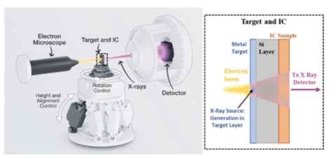
The proposed instrument (left) utilizes a focused electron beam incident on a metal target and integrated circuit (IC) or semiconductor sample. Generated x-rays are attenuated by the sample before being detected and used to generate a 3D image. Inset (right) shows a schematic of the metal target and sample. The target is deposited directly onto the sample, resulting in a micrometer-scale source-to-sample distance. This achieves ultra-high geometric magnification while maintaining a relatively small sample-to-detector distance for improved detected flux and solid angle of collection. This approach removes the need for x-ray optics, which become increasingly inefficient at higher x-ray energies.
Industry roadmaps identify the characterization of nanoscale subsurface feature shape and composition as a measurement need for the semiconductor industry. However, IC interiors are difficult to probe post-manufacturing due to the presence of many close-packed and nanoscale subsurface features, of multiple material compositions spread over square millimeters of chip area.
X-ray computed tomography (CT) is an industry staple for 3D characterization of subsurface feature size and shape. The state-of-the-art in spatial resolution is achieved at synchrotron beamlines, but is not readily accessible compared to compact, laboratory-scale instruments.
Improved characterization of subsurface features will increase U.S. competitiveness in novel IC development and enhance U.S. supply chain security.
This project will develop an x-ray CT instrument capable of 3D, element-sensitive imaging from the micrometer to the nanometer-scale and over IC chip-relevant scan areas. This represents new capabilities for characterizing subsurface features for both manufacturing and security applications, improving detection of physical defects, material contamination, and malicious tampering.
These new measurement capabilities will extend NIST’s influence in semiconductor characterization while fulfilling a high impact measurement gap in the semiconductor ecosystem. Improved characterization of subsurface features will lead to improved quantification of fabrication or packaging-based defects, enabling advances in IC technology. It will also give U.S. security agencies a unique capability to identify hardware trojans or other forms of malicious tampering.