Summary
Atom probe microscopy was developed over 50 years ago; however, only within the last 15
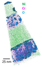
years has the technique begun to see widespread use, due to the convergence of several enabling technological advances. While atom probe tomography holds great promise to deliver atomic-resolution chemically- and isotopically-resolved 3-dimensional images of nanometer-scale volumes of material, much measurement science is needed before the technique can realize its full potential. Atom probe tomography can therefore be classified as an emergent materials characterization technique.
Our laboratory seeks to understand the key factors limiting measurement accuracy in atom probe quantitative analyses. We explore and develop analysis tools and methods to improve measurement accuracy in both chemical and isotopic analyses.
Description
Isotopic Analysis for Isotopic Geochemistry, Nuclear Safety, and Materials Science:
Atom probe tomography has a significant advantage over other forms of mass spectrometry, which typically have a combined efficiency < 5%, in terms of ionization and detection efficiency. Commercial atom probe instruments currently provide an ionization efficiency of about 100% and a detection efficiency < 80%. Therefore, atom probe mass spectrometry can theoretically achieve a level of measurement uncertainty that would require an analysis volume roughly > 10 x larger with another mass spectrometry technique. Further, atom probe samples can be readily extracted from site-specific sub-micrometer regions of larger specimen materials. Atom probe tomography is, thus, increasingly finding use in the analysis of nanometer-scale volumes of material in the fields of isotope geochemistry, nuclear safety, and materials science. However, there is an open question within the community as to the reliability of chemical and isotopic analyses performed via the atom probe. Often, quantitative analyses performed with the atom probe can only be trusted if the chemical or isotopic composition is known a priori, or if additional correlative information from an independent analysis technique is available to lend confidence to the results.
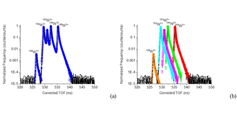
We are exploring the accuracy of quantitative isotopic abundance measurements via atom probe mass spectrometry to better understand the causes of some limited sources of bias. Since isotopic analysis is, in many ways, the simplest form of analysis we can do in the atom probe, these analyses provide a way of testing the basic assumptions used for quantitative analysis and for assessing the ultimate accuracy of the technique. Our goal is to develop accurate, repeatable, and mathematically defensible isotopic analysis methods for the broader community.
Analysis of Key Dopant Elements in Silicon:
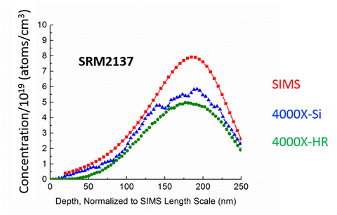
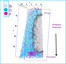
The ability to reproducibly pinpoint exact dopant locations with sub-nanometer accuracy is rapidly becoming critical to successful device fabrication, quality control, and performance. Atom probe tomography can, in principle, deliver atomic-resolution, chemically- and isotopically-resolved 3-dimensional images of device structures. The high combined ionization and detection efficiency of the atom probe makes the technique especially amenable to nano-scale analysis volumes containing few atoms. Further, the combined efficiency remains nominally constant across the full range of the mass spectrum, requiring no matrix corrections or sensitivity factors for quantitative analysis. Atom probe tomography thus holds great promise as a technique that may be able to provide the sub-nanometer spatial resolution and analytical sensitivity required to meet the continuously evolving characterization needs of the semiconductor industry. Over the years, we have partnered both internally (NIST) and externally (SEMATECH, CAMECA, Intel, University of Maryland, and Harvard University) to explore the current limits of dopant profile measurements via atom probe tomography - Arsenic (ca. 2013), Boron (ca. 2015), and Phosphorus (ca. 2017). Each dopant has presented a different challenge for accurate quantification. Accurate arsenic depth profiles were reported. Boron signal loss was confirmed, at levels reported by the instrument manufacturer and by semiconductor industry contacts. The boron signal loss was found to be associated with multi-hit detection events. In a 2017 interlaboratory study on measuring phosphorus in silicon, as organized by Harvard University, the standards-based approach employed by NIST-Gaithersburg outperformed all other participant laboratories and produced measurements roughly 2x more accurate, as judged by percent relative error. Our goal is to perform the measurement science required to develop standardized guidelines for dopant analysis by atom probe tomography.
Development of Quality and Performance Metrics:
We have described atom probe tomography as an emergent characterization technique. As such, the community is only just beginning to create community-wide, consensus-based documentary standards, standard methods, and guidelines for performing analyses.
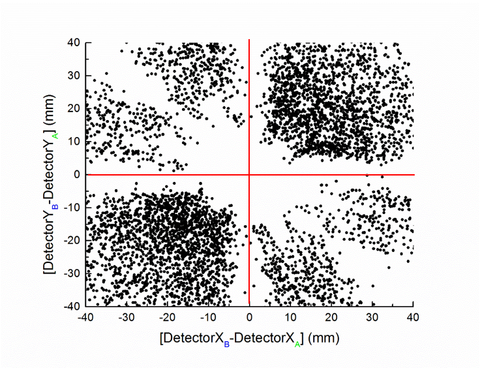
The measure of peak width in a mass spectrum is one of the most important metrics by which mass spectrometer performance is measured. For time-of-flight mass spectrometry, evaluation of the mass resolving power is subject to certain constraints, i.e. constant accelerating voltage, constant flight path length, and constant mass-to-change state ions. In the atom probe, neither the flight path length nor the accelerating voltage remains constant during data acquisition making calculation of a meaningful mass resolving power difficult. NIST had partnered with CAMECA to explore different methods of evaluating the mass resolving power. A measurement approach, that may lead to a test method, has been developed which should allow analysts to generate reproducible mass resolving power values as a spectrometer performance metric. Similarly, NIST has been exploring methods for evaluating atom probe ion detector performance.
Exploring Artifact Signals in Mass Spectra:
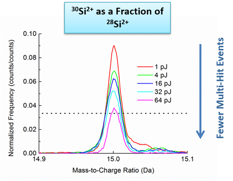
Atom probe tomography mass spectra contain artifacts. Some of the artifacts are commonly observed, such as the background spectrum and the tails on peaks. Other artifacts are more subtle, such as the effects of DC field evaporation, ion feedback, and multi-hit detection events. However, all artifacts affect the ability of the analyst to interpret and quantify mass spectra. Obtaining a deeper understanding of the origins of these artifacts should lead to more accurate quantitative analyses and help provide a more robust understanding of the behavior of the instrument. Further, identifying artifacts in the mass spectrum, and their origins, are necessary steps before attempts can be made to ameliorate the effects of the artifacts or to recover information that would otherwise be lost to an artifact.
Atom Probe Tomography and Microscopy 2018:
The 56th International Field Emission Society meeting was held at NIST-Gaithersburg (June 10–June 15). The biennial International Field Emission Symposium, recently renamed Atom Probe Tomography and Microscopy (APT&M), has been in existence since 1952. APT&M is the premier international gathering of interdisciplinary researchers in the fields of high field nanoscience and atom probe microscopy. The six-day meeting had 215 registered attendees representing institutions from 17 different countries. The program included 164 oral presentations (17 invited) and 94 poster presentations.
|
Isotopic Analysis for Isotopic Geochemistry, Nuclear Safety, and Materials Science:
Analysis of Key Dopant Elements in Silicon:
Quality and Performance Metrics in Atom Probe Tomography:
Exploring Artifact Signals in Mass Spectra:
Atom Probe Tomography and Microscopy 2018:
|

