
Official websites use .gov
A .gov website belongs to an official government organization in the United States.
Secure .gov websites use HTTPS
A lock (
) or https:// means you’ve safely connected to the .gov website. Share sensitive information only on official, secure websites.
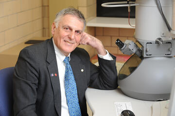
The Person behind the Nobel Prize: Dan Shechtman
Dan Shechtman was born on January 24, 1941 in Tel Aviv, a city on the Mediterranean coast of what was then Palestine and in 1948 became the state of Israel. His mother’s parents had immigrated to Palestine from Ukraine in the early 1900s, and his grandfather, Zeev Ashur, set up the first Jewish printing house in Palestine. They worked with people who would later become prominent in Israeli politics, including David Ben-Gurion, the nation’s first prime minister, and Isac Ben Zvi, the second president of the state of Israel.
Shechtman’s father came to Palestine in the 1930s, also from Ukraine, and went into printing after marrying Shechtman’s mother. They moved several times during Shechtman’s childhood, but never far from Tel Aviv.
“I was really a scientist since a very early age. I was interested in how things work,” Shechtman says. “Maybe the gift that made me a young scientist was a gift from my grandfather, who bought me a magnifying glass. I was running around with this magnifying glass, looking at everything small—insects, little flowers, grain of sand … I fell in love with the world of small things. And this carried me a long way.”
By the time Shechtman finished high school, however, he had developed a different dream—to be an engineer. He was inspired by Cyrus Smith, a railroad engineer with many skills who was the hero of the French author Jules Verne’s 1874 book, “The Mysterious Island.”
“I wanted to be like him,” he recalls.
Shechtman was also trained as a sharpshooter during high school, and like every Israeli citizen or permanent resident, he completed a mandatory 2.5-year-long military service after graduation. He then moved to Haifa, an hour’s drive north of Tel Aviv, to study mechanical engineering at the Technion, Israel’s first science and engineering university. When he finished his bachelor’s degree in 1966, he found few jobs available because of a deep recession in Israel. So he stayed on for a master’s degree and earned a living as a teaching assistant.
By the time Shechtman received his master’s degree, the economic situation had improved, and he was offered what he calls a “wonderful” engineering job, but he was no longer interested. He had rediscovered his childhood fascination with science, and decided to stay for a Ph.D. in materials science at Technion, which he earned in 1972. During his Ph.D. program, Shechtman worked on studying microstructural changes in titanium alloys during fatigue loading—in which forces are repeatedly applied to the alloys, eventually weakening them. He did the work with David Brandon, who introduced a new piece of equipment to Technion—the transmission electron microscope, or TEM.
“When I chose [Brandon] to be my advisor, in effect I chose transmission electron microscopy, and I became an expert in transmission electron microscopy, not in developing the microscope, but in using the microscope,” Shechtman says.
Transmission electron microscopy was invented in 1931 by German scientists Max Knoll and Ernst Ruska, the latter of whom received the Nobel Prize in Physics more than 50 years later in 1986. The technique works by bouncing electrons—one of the fundamental particles that make up atoms—off of a material and recording the electrons’ positions on a detector screen. This is known as electron diffraction. Though electrons are often thought of as particles, according to quantum mechanics—the physics that governs the atomic scale—they are also waves, with wavelengths a hundredth to a thousandth that of visible light. Such short wavelengths mean electrons can create images of objects and structures far smaller than those that light microscopes can—down to the level of a single atom.
After earning his Ph.D., Shechtman sent letters of application for 100 postdoctoral research positions, and received two offers. The more appealing one was from the Aerospace Research Laboratories at the Wright-Patterson Air Force Base in Dayton, Ohio, so Shechtman, his wife and their then two children took off for the American Midwest. There, he used his TEM skills to study compounds of the metals aluminum and titanium, with the goal of developing strong, lightweight materials for aircraft components.
While at Wright-Patterson, he met a well-known materials scientist named Martin Blackburn.
“In one of my conversations with him, I asked him, ‘What’s in the future for materials science?’” Shechtman says. “He said, ‘I think rapid solidification’”—techniques for causing a mixture of metals or other elements to solidify from a liquid very quickly, often leading to new materials with interesting properties. “So I chose to develop in that direction.”
In 1975, Shechtman moved back to Haifa to take a permanent position at Technion. He continued studying rapidly solidified materials with transmission electron microscopy. The microscope’s electrons can penetrate only very thin samples—as thin as one-tenth of a millionth of a meter. So Shechtman pioneered an electrochemical technique to slice powders produced by rapid solidification into thin sheets that he could study with the TEM.
In 1979, he got a visit from John Cahn, a well-known and respected materials scientist at the National Bureau of Standards (NBS), the agency that later became NIST. They had met on an earlier visit of Cahn’s to Technion in the late 1960s. This time, Shechtman had something special to show Cahn: the technique he used to produce thin TEM specimens from metallic powders. Cahn said, “We tried to do that for two years, and wow, you do it just like that. We need you. Why don’t you come for a sabbatical to NBS?” Shechtman recalls. “I said, that would be great.”
So in 1981, Shechtman, his wife and by then four children headed back across the Atlantic for a two-year position as a visiting researcher. Though his appointment was technically at Johns Hopkins University in Baltimore, Maryland, Shechtman was hosted by Cahn and worked at NIST’s Gaithersburg, Maryland, campus.
“One thing about Danny you may not know—he’s also a good jeweler. I remember him making nice jewelry when he was here [at NIST]. One time he was using titanium, and oxidizing it by heating it very carefully. You can get many different colors as a consequence of the reflection patterns he created. He did very nice jewelry work here.”
– Robert Shull, NIST Fellow, Materials Science and Engineering Division