
Official websites use .gov
A .gov website belongs to an official government organization in the United States.
Secure .gov websites use HTTPS
A lock (
) or https:// means you’ve safely connected to the .gov website. Share sensitive information only on official, secure websites.
Summary
Electron-beam lithography enables fine control of nanostructure features that form the basis of diverse nanotechnologies. The Nanostructure Fabrication and Measurement Group advances lithographic accuracy at the nanometer scale and develops processes to fabricate innovative devices and standards in physical domains ranging from photonic to fluidic.
Description
Electron-beam lithography allows fine control of nanostructure features that form the basis of diverse device technologies. Lateral resolution of 10 nm, placement accuracy of 1 nm, and patterning fields of 1 mm are all possible. However, achieving these performance metrics depends on many interdependent factors that are specific to the sample – pattern definition and fracturing, substrate and mask materials, pre-exposure and post-exposure processes, alignment feature definition – as well as, critically, details of the operation of the lithography system.
As a core capability, we develop processes that are at or near the limits of conventional electron-beam lithography to advance nanoscale devices and measurement science in a variety of fields, such as: chip-scale frequency combs for precision time-keeping; nonlinear integrated optics for wavelength and quantum frequency conversion; on-chip cavity optomechanical and micro/nano-electromechanical systems for sensing, transduction and non-linear dynamics studies; quantum photonic integrated circuits with non-linear and quantum emitter light sources for quantum information; metasurfaces from UV to infrared for trapping and probing atoms and ions, polarimetry, imaging, and spatiotemporal ultrafast laser pulse shaping; optical microscopy standards for aberration correction.
To advance our fundamental capabilities of electron-beam lithography, we are developing methods to better control, measure, and understand fabrication processes. To reduce the barrier to entry of electron-beam lithography and to improve control of pattern accuracy, we created the Nanolithography Toolbox. This freely available software allows the rapid design of complex multilayer patterns through a simple and well-documented scripting language. To achieve better lateral resolution, we are developing physical models to simulate the exposure of electron-beam resist to optimize patterning processes, and we are advancing methods of scanning-electron microscopy and scanning-probe microscopy to measure edge roughness. To improve pattern placement, we are applying electron-beam lithography to pattern standards for correlative atomic-force microscopy and super-resolution optical microscopy, with accurate localization with high throughput enabling characterization and optimization of process parameters. Such measurements create a positive feedback loop of making and measuring nanostructures.
Highlights
Highlight: The Nanolithography Toolbox
The accuracy of lithographic design is critical to nanofabrication in general, and to electron-beam lithography in particular. Layout design is commonly performed using semiconductor-standard software. However, such software is not ideal for nanophotonic, nanoplasmonic, nanofluidic, and nanomechanical device designs, which commonly feature curved geometries with aggressively scaled dimensions. To efficiently design such geometries, we have developed and are updating the Nanolithography Toolbox, a freely available and platform-independent computer-aided design software package for creating and streaming complex shapes to the standard GDSII layout format. Using parameterized shapes as building blocks, the Toolbox allows users to rapidly design and layout nanoscale devices of arbitrary complexity through scripting and programming. The Toolbox includes a large and expanding library of parameterized shapes for nanophotonic and nanomechanical devices, all documented in a comprehensive manual. To date, the Toolbox has had in excess of 3,500 downloads, and is currently in use by prominent industrial stakeholders including 3M, Google X, Oculus/Facebook, Thorlabs, and Roche.
- Balram, et al., The Nanolithography Toolbox, J. Res. Natl. Inst. Stand. Technol. 121 (2016). Download here.
- Arhberg, et al., Handheld real-time PCR device, Lab on a Chip 16 (2016)
Highlight: Electron-beam lithography for heterogeneous nanophotonics
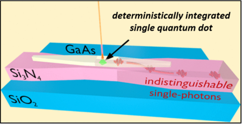
Self-assembled quantum dots in III-V semiconductors are promising sources of single photons for quantum technologies. Nanophotonic hosting geometries are the key to optimally collect photons emitted by a single quantum dot. We have designed and fabricated GaAs nanophotonic structures capable of efficiently launching single photons emitted by embedded InAs quantum dots into silicon photonic integrated circuits. While silicon photonic circuits are promising for large-scale quantum systems, our method supplies a critical functionality that is unachievable with silicon alone. A challenge is that the self-assembly of quantum dots yields limited control over dot spatial location. Critically, a quantum dot requires precise positioning within its hosting geometry for optimal performance. To meet this challenge, in collaboration with the Technical University of Berlin, we used cryogenic cathodoluminescence imaging to locate a single quantum dot in a thin GaAs film bonded to a Si3N4 wafer. We performed unconventional in situ electron-beam lithography to define a nanophotonic hosting geometry precisely aligned to a specific quantum dot. After etching of the III-V layer, we used conventional electron-beam lithography to define a precisely aligned interfacing Si3N4 photonic circuit. Our deterministically generated single quantum-dot device allowed us to demonstrate, without precedent, the generation of triggered and indistinguishable single-photons in a Si3N4 photonic circuit.
- Davanco, M. et al., Heterogeneous integration for on-chip quantum photonic circuits with single quantum dot devices, Nature Communications 8 (2017)
- Schnauber, P. et al., Indistinguishable Photons from Deterministically Integrated Single Quantum Dots in Heterogeneous GaAs/Si3N4 Quantum Photonic Circuits, Nano Letters 19 (2019)
Highlight: Electron-beam lithography for reproducible nanophotonics
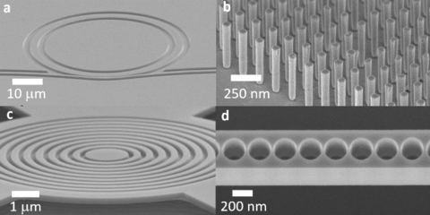
Nanophotonic structures enable control of the interaction of light and matter, allowing observation and application of linear, non-linear, quantum optical, and optomechanical phenomena on chip. This control is possible through strong confinement of light in nanostructures. However, dimensional variations of less than 10 nm can lead to large variations in light propagation. Therefore, the fabrication process requires care to achieve reproducible performance – a real necessity not only for applications, but also for cycles of device development. The core capability of the Division in electron-beam lithography allows routine demonstration of such control in creating nanophotonic devices for various applications. In practical terms, this means that the Division is able to design, through electromagnetic simulations, a nanophotonic structure, fabricate and then measure devices in a virtuous cycle, thus achieving reproducibly high performance. An example is the development of Si3N4 microring resonators for optical parametric oscillation, for which engineered guided wave dispersion as a function of wavelength and low propagation losses are essential. Variation of microring width by less than 10 nm allowed control and observation of parameteric oscillation over a wide range of visible wavelengths, from red to green.
- Lu, X. et al., Milliwatt-threshold visible-telecom optical parametric oscillation using silicon nanophotonics, Optica 6 (2019)
- Lu, X. et al., On-chip optical parametric oscillation into the visible: generating red, orange, yellow, and green from a near-infrared pump, Optica 10 (2020)
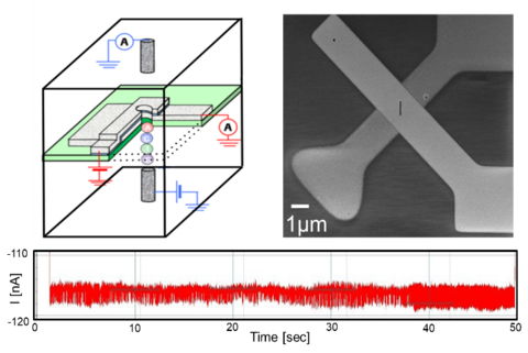
Highlight: Electron-beam lithography for molecular recognition and sequencing
Detecting, identifying, and sequencing biopolymers is essential to developing new capabilities to diagnose and treat disease. It is particularly important for DNA, considering the genetic aspects of deceases such as cancer. Nanoscale metal–insulator–metal (MIM) tunnel junctions can detect single molecules by molecular mediation of resonant tunneling. We have worked with F. Hoffmann-La Roche Ltd., an industrial stakeholder, to fabricate Pt/Al2O3/Pt junctions with nanopores patterned by electron-beam lithography on top of free-standing Si3N4 membranes separating two microfluidic reservoirs. We combined electron-beam and optical-projection lithography to define and overlay nanostructures, advanced ion-beam deposition, and ion-beam and reactive-ion plasma etching tools to make prototype devices and demonstrate the feasibility of biomolecular detection. The process required the precise alignment of electric-beam lithography to pattern the nanopores at the center of nanoscale junctions. We identified biomolecules by their tunneling currents as they translocate through the nanopore from one microfluidic reservoir to the other. We have been able to observe translocation of short DNA oligomers and identify various organometallic complexes by analyzing power-spectral densities of tunneling-current noise.