Official websites use .gov
A .gov website belongs to an official government organization in the United States.
Secure .gov websites use HTTPS
A lock (
) or https:// means you’ve safely connected to the .gov website. Share sensitive information only on official, secure websites.
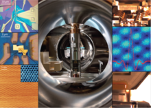
Scanning Probe Metrology
Summary
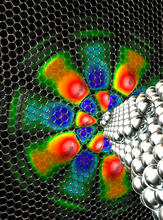
Underlying all information transfer and computation involves the movement and detection of electrons, which are the subatomic particles found in all atoms that make up materials. Understanding how electrons travel, assist in binding atoms together to make materials, and how they distribute themselves in different materials is central to understanding how the world works. Measuring the properties of atoms and electrons in materials necessarily benefits from measurements that are at the smallest scale possible in the atomic regime and use the quantum nature of electrons themselves as a probe. The program in scanning probe metrology does this by developing quantum measurement tools and methods that are required to reveal the quantum phenomena in new materials and devices at the atomic scale to harness them for applications in metrology, sensing, and quantum information science. The capabilities involve quantum tunneling of electrons, quantum force, quantum spin resonance, and quantum transport measurements in multi-modal instruments aimed at the atomic level. The instruments and measurements are made possible by custom designed world-class instruments, unparalleled outside of NIST, operating at ultra-low temperatures down to 10 mK (0.01 K) in ultra-high vacuum and with applied magnetic fields up to 15 T. This allows quantum wavefunctions to be mapped with atomic scale resolution and electron energy levels to be resolved with μeV energy resolution. The measurements are closely coupled with fabrication facilities for molecular beam epitaxy of various materials as well as nanofabrication of heterostructed devices.
DESCRIPTION
The Quantum Nanoelectronics Group has four themes in Advanced Development of Scanning Probe Metrology Instrumentation and Measurements focused on Quantum Nanoelectronics.
Advances in SPM Instrumentation
Designing Advanced Scanning Probe Microscopy Instruments


THE TEAM