Official websites use .gov
A .gov website belongs to an official government organization in the United States.
Secure .gov websites use HTTPS
A lock (
) or https:// means you’ve safely connected to the .gov website. Share sensitive information only on official, secure websites.
Summary
The interest in using graphene as an electronic material arises in large part from the high speed with which electrons move through the material — approximately 100 times faster than in the silicon used in almost all modern electronic devices. Graphene is a single atomic layer of carbon with the thickness of a single carbon atom, making it ideal for small electronic devices like transistors or sensors. Graphene can be patterned using standard semiconductor lithography techniques and can serve as both the active element of the electrical component and as the "wires" or connections to other parts of the electrical circuit. Many of the notable properties of graphene stem from its unique electronic structure and topology. The goal of this project is to determine the unique structural and electrical properties of graphene using atomic-scale local probe measurements.
Description
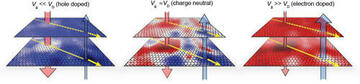
Two remarkable features of graphene that are opening avenues to multiple applications are its high transport carrier mobility and the broad tunability of its electronic properties. Graphene charge carriers can be tuned continuously from negative carriers (i.e., electrons) to positive carriers (holes). Separating the point between the negative and positive carriers is a neutrality point where the net charge goes to zero. This condition is called the Dirac point, named after the Dirac theory used to describe graphene charge carriers. Arising from the Dirac point is a linear dispersion of the energy vs momentum of the charge carriers.
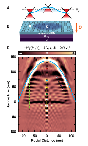
To perform measurements on graphene devices, NIST researchers fabricated a representative electrical device. A typical semiconductor device is a complex "sandwich" of alternating conducting, semiconducting, and insulating layers and structures. To perform experiments on graphene devices, the NIST team fabricated structures with a single atomic sheet of graphene and another conductor separated by an insulating layer. When the bottom conductor is charged, it induces an equal and opposite charge in the graphene layer, and in this way the carriers can be switched from electrons (negative charges) to holes (positive charges). To determine how the graphene carriers are affected by the substrate insulators, NIST researchers used custom-designed scanning probe microscopes. A unique feature of the NIST microscopes is the ability to optically align the SPM probe tip to the very small active graphene area on the device, which may be as small as tens of micrometers in length. Once aligned, the microscope is cooled to liquid He temperatures (4 K) and tunneling microscopy and spectroscopy measurements are performed to probe the graphene carriers on the atomic scale. NIST researchers have used atomic-scale measurements, scanning tunneling microscopy, and scanning tunneling spectroscopy to understand the various properties of graphene related to its electronic structure.
Graphene Linear Dispersion
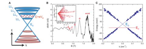
The energy spectrum of graphene's charge carriers is very different from ordinary metals and semiconductors. The conduction and valance bands meet at conical points, where the carriers have an energy that is linear in momentum, giving rise to a zero effective mass [Fig.1(a)]. This dispersion is called the Dirac cone because the equation describing the motion of the carriers resembles the Dirac equation for relativistic particles. At the conical point, called the Dirac point, the density of carriers is zero in an ideal graphene lattice. When a magnetic field is applied perpendicular to the graphene sheet, the charge carriers undergo cyclotron motion and condense into sharp quantized energy levels, called Landau levels [Fig. 1(a)]. A hallmark of graphene that results from the unique linear dispersion is that the energy spacing between the Landau levels is not constant but varies with energy, and a special state comes into existence at the Dirac point, where there were no carriers when the magnetic field was not applied. The linear dispersion can be obtained by measuring tunneling magneto-conductance oscillations [Fig. 1(b)]. These magneto-oscillations are distinctly different from traditional Shubnikov–de Haas oscillations (SdHOs) in transport measurements, as they measure the band structure properties at variable tunneling energy rather than a single energy at the Fermi surface. Using the TMCO measurements, we map the low-energy dispersion of graphene with an energy resolution of 2.8 meV, and we extend these measurements of energy versus momentum into the empty electronic states that are inaccessible to photoelectron spectroscopy [Fig. 1(c)].
Charge Puddles in Graphene
The interaction of graphene with the underlying substrate can create charge puddles, which create potential inhomogeneities that induce a random doping profile in the graphene in response to the charge puddles. To get at the root cause of these inhomogeneities, NIST researchers developed a density mapping tunneling spectroscopy measurement to observe the nanoscale spatial variations in carrier density. In this method, the tunneling conductance is measured as a function of energy at constant gate potential, and then the spectra are repeated with a small incremental change in gate potential. The resulting data is displayed in a map, showing a rich variety of detail that cannot be gathered by a single tunneling spectrum.
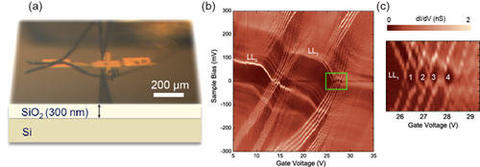
Using these methods, the NIST team determined that the silicon oxide substrate potential fluctuations are interrupting the orbits of the electrons in the graphene, creating wells where the electrons and holes pool and reducing their mobility. The resulting p-n junctions (neighboring electron and hole regions) only localize the graphene carriers weakly due to the ability of graphene carriers to penetrate potential barriers. However, the NIST team found a dramatic change when a magnetic field was applied. The electrons lack the energy to scale the barriers of resistance created by energy gaps between the Landau levels, and settle into isolated pockets of graphene quantum dots: nanometer-scale regions that confine electrical charges in all directions. The Coulomb charging of the quantum dots was observed as a diamond structure in the gate maps when the Landau levels cross the Fermi energy [Fig. 2(c)].
NIST researchers found even more complicated nanoscale behavior caused by substrate interactions in bilayer graphene (two stacked graphene layers). It has been known for some time that bilayer graphene acts more like a semiconductor with a band gap when immersed in a perpendicular electric field. Just like single-layer graphene, the insulating substrate induces electron and hole puddles to form. However, in bilayer graphene, both electron and hole puddles are deeper on the bottom layer because the bottom layer is closer to the substrate. This difference in puddle depths between the layers creates a random pattern of alternating charges and the spatially varying band gap [Fig. 3], which was difficult to detect when the bilayer band gap was measured with macroscopic measurements.
Berry Phase and Circular Graphene Resonators
Associated with the Dirac point in the graphene dispersion is a source for Berry curvature, which gives rise to a Berry phase when momentum space orbits encompass the Dirac point. The Berry phase is the geometric phase accumulated as a quantum state evolves adiabatically around a cycle according to Schrödinger’s equation. Graphene is a rare example where the Berry phase can alter the energy spectrum of the charge carriers. Because of the pseudo-spin-momentum locking, the Berry phase associated with a quantum state can take only two values, 0 or 𝜋, which gives rise to the unconventional “half-integer” Landau-level structure in the quantum Hall regime.
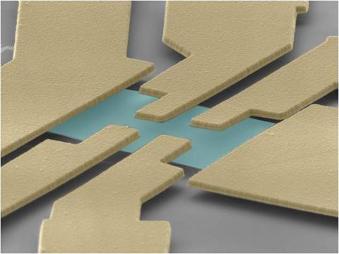
Using graphene devices, NIST researchers have shown that a Berry phase switch can be engineered in graphene resonators. Graphene resonators confine Dirac quasiparticles by Klein scattering from p-n junction boundaries. Circular resonators were produced by a scanning tunneling microscope (STM) by creating a fixed charge distribution in the substrate, generated by strong electric field pulses applied between the tip and graphene/boron nitride heterostructure [Fig. 4].
The Berry phase switch of the energy eigenstates of the resonator are shown in Fig. 5 where we probe the magnetic field dependence of the 𝑚 = ±1/2 resonator states (Fig. 5A) for the states 𝑛 = 1 to 𝑛 = 5, corresponding to the energy range indicated by the yellow dashed line in Fig. 4D. We see the degenerate 𝑚 = ±1/2 states in the center of the map at 𝐵 = 0, corresponding to the states seen in the center of Fig. 4D at 𝑟 = 0. However, as the magnetic field is increased, new resonances suddenly appear between the 𝑛th quantum levels, where none previously existed. The spacing between the new magnetic field–induced states, 𝛿𝜀𝑚, is about one-half of the spacing, ∆𝐸, at 𝐵 = 0. Figure 5C shows a magnified view of the 𝑛 = 4 quantum state where new states appear at a critical field of 𝐵𝑐 = ±0.11 T.
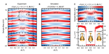
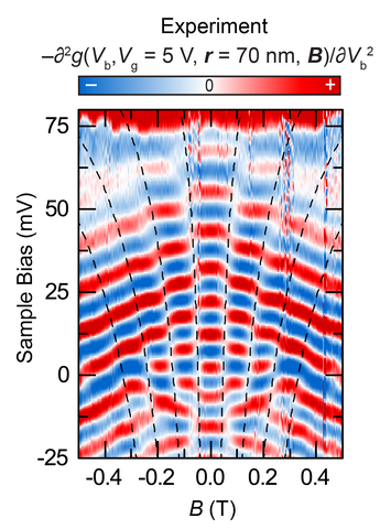
A semiclassical analysis of the Berry phase switch predicts that the critical field should scale with the orbital quantum number 𝑚, as 𝐵𝑐 = 2ħ𝑚𝜅 / 𝑒ε where 𝜀 is the energy of the orbit. Access to higher m states were made with measurements away from the center of the resonator and show excellent agreement with the above critical field expression, as shown in Fig. 6.
Spatial vs Magnetic Confinement in Graphene Circular Resonators
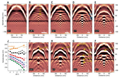
Energy quantization due to quantum confinement takes place when the particle’s de Broglie wavelength becomes comparable to the system’s length scale. Confinement can arise through spatial constraints imposed by electric fields or through cyclotron motion induced by magnetic fields. Graphene circular resonators offer a platform to examine the transition from spatial confinement using electrostatic potentials to magnetic confinement introduced by cyclotron motion. Figure 7 shows the intricate evolution of the resonator quantum states as the magnetic field is steadily increased. The first critical field is reached by 0.25 T, where the ±𝑚 degeneracy is lifted owing to the turn-on of a 𝜋 Berry phase, as discussed above and as seen by the doubling of the anti-nodes at 𝑟 = 0 (arrows in Fig. 7B). The onset of the transition into the quantum Hall regime can be observed at 𝐵 = 0.5 T (Fig. 7C). Here, states in the center of the resonator start to flatten out, have increased intensity, and shift lower in energy. Beginning at 𝐵 = 1 T, various interior resonator states (arrows in Fig. 7D) merge into the N = 0 Landau level (LL(0)). With progressively higher fields, the number of QD resonances decreases as they condense into the flattened central states, forming a series of highly degenerate LLs (Fig. 7, F to I).
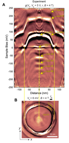
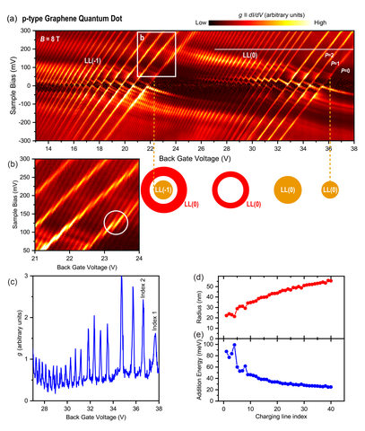
The flattened LLs form a wedding-cake-like structure in the resonator comprising a series of compressible and incompressible disks and rings of an electron fluid. The incompressible and compressible rings become considerably clearer in a higher magnetic field. The experimental spectral map in Fig. 8A shows the LLs becoming flat in the central region of the QD, even though the bare external electrostatic potential is concave, and then they progress sharply to a new energy level as new LLs become occupied, forming a wedding cake-like structure. Here LL(N), N = –5 to 2 can be observed as plateaus in the center of the QD (Fig. 8A). Both LL(0) and LL(-1) cross the Fermi level at zero bias as indicated by the yellow lines, forming a LL(-1) compressible disk in the center and an outer LL(0) compressible ring separated by an incompressible ring, as shown in the Fermi-level spatial map in the x-y plane (Fig. 8B). We observe Coulomb charging of these LLs as charging lines intersecting the LLs at the Fermi level and progressing upward at sharp angles in Fig. 8A. These lines correspond to a quartet of rings in Fig. 8B. The charging of the compressible regions occurs in groups of four, reflecting the four-fold (spin and valley) graphene degeneracy.
Single-electron Charging of Compressible Landau Level Islands in Graphene
Applying even higher magnetic fields to the graphene resonators results in isolated incompressible rings that behave as quantum dots (QD), where single-electron charging events can be well studied. Figure 9(c)-(f) show the STS dI/dV signal acquired in line spectroscopy measurements through p- and n-type QDs ((c) and (d), respectively) and in x-y raster scans at fixed bias ((e) and (f), respectively). In all panels the gate was set within the double-QD regime, where LL(-1) and LL(0) cross 𝐸𝐹 within the well. In the raster scans, the charging features are due to the effect of spatially-dependent tip gating and take the form of concentric rings. The two LLs which are being charged each have their own set of concentric rings; charging rings of LL(-1) and LL(0) are indicated by dark and light grey arrows respectively. In the n-type dot (Fig. 1(f)) the centers of the two sets of charging rings have spatially separated centers and can be readily distinguished. In the line spectroscopy measurements (Fig. 9(c) and (d)), the two sets of charging peaks appear as series of nested quasi-parabolic “U”-shaped curves whose vertical spacing Δ𝑉𝐵 can be used to estimate the charging energy of its respective QD (see Fig. 2 et seq.). Within each potential well the two sets of charging “U”s can be distinguished by their curvature and spatial extent: those belonging to the outer LL(-1) are broader, flatter, and more closely spaced in Δ𝑉𝐵, while those belonging to the inner LL(0) are steeper and more widely spaced.
Both types of charging curve resemble the features observed in scanning gate microscopy of QD systems, and can be explained as an induced charge in the QD, Δ𝑞 = 𝐶𝑡𝑖𝑝(𝐫)Δ𝑉𝑡𝑖𝑝, where Δ𝑉𝑡𝑖𝑝 is the contact potential difference between the tip and graphene minus the sample bias 𝑉𝐵. The tip capacitance 𝐶𝑡𝑖𝑝 should be regarded as an effective capacitance that derives from the interaction of the spatially-varying tip potential with the QD potential well, as screened by the successive partially-filled LL rings. Importantly, since the electron density per filled LL in the quantum Hall regime is fixed, the charging (dis-charging) of the LL quantum dot by the scanning tip is accompanied by growth (shrinkage) of the total occupied area at the Fermi level, and corresponding deformations of the compressible ring, which is its boundary.
By keeping the probe position fixed, single electron charging events can be observed as peaks in the differential conductance vs applied back gate potential 𝑉𝑔 and sample bias 𝑉𝐵. Figure 10(a) shows the spectral 𝑑𝐼/𝑑𝑉𝐵 gate map as a function of 𝑉𝐵 and 𝑉𝑔 with the tip positioned in the center of the confining potential. Here, the map is dramatically dominated by slanted bright lines corresponding to adding a single charge to a LL QD, whereas the usual graphene LL LDOS is observed as a nearly-horizontal intensity modulation of these features. In Fig. 10(a), a single hole is added to LL(0) starting at a large back gate voltage of ≈36 V, initiating a LL(0) QD disk at the Fermi level. As we decrease the gate voltage, additional holes are added and the dot expands: the filled LL(0) rises above the Fermi energy in the dot center, and the compressible part of this LL expands outward, forming a ring. This increase in dot size is inferred from the closer spacing of the charging lines and confirmed by direct STS measurements (Fig. 9(c)). At gate voltage ≈22 V, LL(-1) crosses the Fermi level (see schematic below Fig. 10(a)) and a concentric double-QD is formed. This is indicated by a second series of slanted charging lines that are observed together with the original set from the LL(0) QD; the latter are now finely spaced, reflecting the larger size of the LL(0) QD. These two sets of charging lines display an avoided crossing pattern indicative of a double QD (Fig. 10(b)).