U.S. flag

An official website of the United States government

Official websites use .gov
A .gov website belongs to an official government organization in the United States.

Secure .gov websites use HTTPS
A lock ( ) or https:// means you’ve safely connected to the .gov website. Share sensitive information only on official, secure websites.

Integer and Fractional Quantum Hall Effect

Summary

The physics of the quantum Hall effect (QHE), discovered in 1980, formed the basis of the initial concepts in quantum topological matter. The QHE also forms the basis for the resistance standard in the International System of Units (SI), which is central to the NIST mission space. The QHE effect results when a two-dimensional electron system (2DEG) is subject to a large magnetic field. Subsequently, the charge carriers undergo cyclotron motion and condense into sharp, quantized energy levels, called Landau levels. Historically, the QHE has been studied in GaAs buried heterostructures, where large mobilities are found in the engineered 2DEG systems. At NIST, our project focus has been the study of the QHE and FQHE in graphene systems, where the larger cyclotron energies facilitate a route towards a newer, higher temperature resistance standard replacing GaAs devices. 

Description

Integer Quantum Hall Effect 

Integer QHE LL
Fig. 1: Graphene electronic dispersion in a magnetic field. (a) Conduction (blue) and valence (pink) bands meet at a conical point with a linear energy-momentum dispersion for graphene. (b) The graphene carriers condense into narrow energy levels (Landau levels) when placed in a perpendicular magnetic field, B. (c) Direct measurement of graphene Landau levels with high resolution scanning tunneling spectroscopy. Reference, https://www.science.org/doi/10.1126/science.1171810
Credit: NIST

Graphene is a unique 2DEG system that is exposed at the surface and can be probed with scanning tunneling measurements.  A hallmark of graphene that results from the unique linear dispersion is that the energy spacing between the Landau levels is not constant but varies with energy, and a special state comes into existence at the Dirac point, where there were no carriers when the magnetic field was not applied (see Fig. 1). The cyclotron motion of the carriers can be used in scattering experiments to investigate how electrons travel in graphene and interact with defects, the lattice, and other charge carriers. This information is essential to fully exploit graphene for future device applications.

This project is developing methods to measure the energy spectrum of graphene's charge carriers in applied magnetic fields and to determine the fundamental interactions among graphene's charge carriers with defects, lattice structure, multilayer effects, and many-body interactions. Since graphene is an exposed two-dimensional electron system, every atom is a surface atom that can be probed directly using modern scanned probe microscopy techniques. This accessibility is in contrast to traditional two-dimensional electron systems, which are buried below the surface in semiconductor heterostructures. At the NIST, we have developed unique scanning probe microscopy systems that operate in high magnetic fields and at cryogenic temperatures, enabling very high energy resolution spectroscopy.  

Quantum Hall Edge States 

Carrier density-dependent scanning probe measurements are made using applied gate potentials in 2D fabricated graphene heterostructures. Figure 2a and b shows a 2D graphene heterostructure where two buried graphite gates define a local p-n junction potential. This allows electrostatically defined quantum Hall edge states to be localized at the p-n junction boundary and accessible with local probe measurements. The potential step across the p-n junction was measured using Kelvin probe force microscopy (KPFM), in a multi-modal cryogenic SPM system.  

Integer QHE AFM Potential
Fig. 2: Graphene quantum Hall device structure. a, Cross-sectional schematic of the layered structure of the graphene quantum Hall device. Two graphite back gates define the Hall bar: a global graphite back gate G2 (blue) and a local graphite back gate G1 (red). Pd/Au contacts are used to apply the sample bias 𝑉B to the graphene layer. b, Optical image of the graphene device. The graphene sheet is indicated by the dashed black contour. The region controlled by the local gate G1 is shown by the dashed red line while the region controlled by the global gate G2 is shown by the dashed blue line. Part of the fan “runway” used to guide the tip to the graphene is seen on the right side of the image. c, Line traces from a Kelvin probe map at 𝐵 = 0 T at the local gate potentials indicated, showing the width and sharpness of the potential boundary due to the use of the graphite back gates in close proximity to the graphene layer. A linear fit to the trace at G1 = -1.95 V (black) over the region bounded by the vertical lines yields a slope of (1.72 ± 0.02) meV/nm, where the uncertainty is one standard deviation from the linear least square fit. d, STM topography of the graphene surface. Dark and bright spots represent the moiré superlattice formed by the graphene sheet and the hBN underlayer. The atomically resolved graphene lattice is visible as the fine mesh in the whole area. Topography is obtained at 𝑉B  = -100 mV and a tunneling current of 300 pA.  Reference https://www.nature.com/articles/s41467-021-22886-7 
Credit: NIST

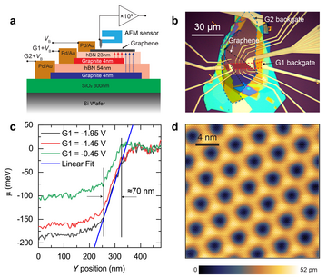
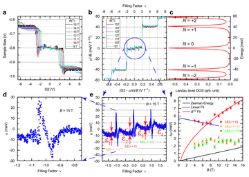
Another advantage of KPFM measurements is the ability to measure the LL spectrum with zero electric field gating since KPFM chemical potential measurements are made at a null force condition. Figure 3 shows KPFM measurements of the graphene LL spectrum, including the breaking of the four-fold degeneracy of the zero LL.  

Integer QHE KPFM
Fig. 3:  Resolving the energies of the four isospin components of the graphene zero Landau level with Kelvin probe spectroscopy. a, Kelvin probe measurements varying the sample bias and simultaneously gates G1 and G2 for measurements made outside the Hall bar area. A staircase of plateaus shows various Landau levels occurring at different chemical potentials for various magnetic fields. b, Chemical potential vs. filling factor given by the data in (a) collapsed onto a universal curve by scaling the sample bias by the graphene Landau level energy field dependence along the vertical axis, 𝐸𝑁 ∝ √𝐵, and by the 𝐵−1 along the horizontal axis to give a density/filling factor axis. Each Landau level is observed by a plateau in the scaled chemical potential. Notice the zero Landau level at zero chemical potential consists of four separate small plateaus indicating the lifting of the four-fold degeneracy. c, The Landau level density of states calculated using the expression in the main text with 𝐵 = 1 T and 𝑣𝐹 = 1.13×10  m/s to fit the locations of the plateaus in (b). d, Blow up of the large up and down excursion in chemical potential at 𝜈 = −1 and 𝐵 = 15 T from (e). e, Blow up of the chemical potential of the zeroth Landau level at 𝐵 = 15 T from (b) showing four individual chemical potential plateaus, labeled 𝜀i, separated by large up/down excursions at the incompressible filling factors, 𝜈 = 0,±1. The red dashed lines indicate the differences in chemical potential ∆𝐸 = (𝜀2 − 𝜀1), (𝜀3−𝜀2), and (𝜀4−𝜀3). f, Energy differences extracted from the chemical potential plateaus in (e) for the 𝜈 = 0, (𝜀3−𝜀2) (red circles) and 𝜈 = −1, (𝜀2−𝜀1) and 𝜈 = +1, (𝜀4−𝜀3) (orange triangles and green squares) filling factors. The values are averaged chemical potential difference values from 𝜈 − 0.75 to 𝜈 − 0.25 of each integer 𝜈, and the error bars correspond to one standard deviation. The solid black line shows the Zeeman energy, 𝑔𝜇𝐵𝐵, with 𝑔 = 2. The solid red line is a fit for 𝜈 = 0 data values to √𝐵 for values ≥ 8 T, and the blue line is a linear fit for 𝐵 values ≤ 8 T. AFM settings: 5.8 nm oscillation amplitude, ∆𝑓 = −450 mHz, 5 Hz bias modulation, except a 1 Hz bias modulation was used for 4 T and 5 T data. Reference https://www.nature.com/articles/s41467-021-22886-7
Credit: NIST

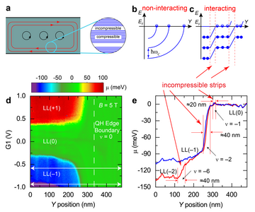
The compressible and incompressible edge channels are also resolved in the KPFM measurements shown in Fig. 4. 

Integer QHE Edge State
Fig. 4: KPFM measurements of incompressible strips. a, Schematic of bulk closed cyclotron orbits with cyclotron energy ħ𝜔𝐶 and edge quantum Hall states leading to compressible and incompressible strips at the device edge boundary. b-c, Schematic of the bending of the Landau levels in a confining potential boundary (b) in a non-interaction picture and (c) in an interacting picture leading to a “wedding cake-like” series of plateaus in Landau levels near the boundary edge. A compressible strip is formed when a Landau level is at the Fermi level, separated by incompressible strips (red dashed lines) during Landau level transitions. d, Kelvin probe map at 𝐵 = 5 T of the chemical potential as a function of Y-position across the quantum Hall boundary (indicated in the black circle in Fig. 2a) and local-gate potential. In the local-gate area, Landau levels from 𝑁 = −2 [LL(-2)] to 𝑁 = +1 [LL(+1)] are seen in the different colored plateaus. AFM settings: 2 nm oscillation amplitude, ∆𝑓 = −2 Hz, and 20 mV sample bias modulation at 1.4 Hz. e, Incompressible strips in the chemical potential are observed in the lines traces at G1 = −0.9 V (red) and G1=−0.6 𝑉 (blue) [white horizontal lines in (d)] corresponding to filling factors 𝜈 = −6, −2, and −1. The transitions separate plateaus between Landau levels, LL(-2) to LL(-1), and LL(-1) to LL(0), confirming the “wedding-cake-like” structure. Reference https://www.nature.com/articles/s41467-021-22886-7
Credit: NIST

Fractional Quantum Hall Effect 

The fractional quantum Hall effect (FQHE) is a hallmark of strong interactions in two-dimensional electron systems in the presence of large magnetic fields. Of particular importance among the number of FQH states are specific even-denominator states, which are expected to exhibit non-Abelian statistics. GaAs quantum well systems have been the main system where FQHE has been traditionally studied. With the advent of graphene 2DEG systems, FQHE states are now accessible with scanning probe measurements. In this project, we are investigating the FQHE in bilayer graphene, which has been shown to host a number of even-denominator states. We use a split gate geometry to define an electrostatic boundary to study FQHE edge states, as shown in Fig. 5.  

Integer QHE Bilayer Graphene Device
Fig. 5: Bilayer graphene device. Optical images of the bilayer graphene device with underlying graphite split gates as fabricated (left) and loaded into the SPM sample holder (right). 
Credit: NIST
Created August 19, 2025, Updated September 2, 2025
Was this page helpful?