
Official websites use .gov
A .gov website belongs to an official government organization in the United States.
Secure .gov websites use HTTPS
A lock (
) or https:// means you’ve safely connected to the .gov website. Share sensitive information only on official, secure websites.
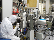
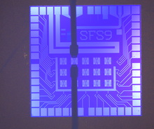
Boulder Microfabrication Facility: Science Impacts
Summary
Groups that are major users of the cleanroom and details of their projects are listed below.
Major USERS
Advanced Microwave Photonics Group
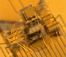
The Advanced Microwave Photonics Group focuses on novel ways to couple quantum electrical and mechanical circuits with an emphasis on problems in quantum information and the limits of measurement. This project takes advantage of superconductivity at low temperatures, Josephson junctions, mechanical elements, and careful circuit design to develop quantum bits (qubits), mechanical and electrical resonators, tunable couplers, and electrical measurement techniques to exploit the fundamental laws of quantum mechanics to improve computing, simulation, and high precision measurements. They use the BMF to fabricate most of their devices.
Superconductive Electronics Group
The Superconductive Electronics Group utilizes the quantum effects of Josephson junctions in specialized superconducting integrated circuits to improve measurement technology and standards for fundamental metrology, such as for dc and ac voltage, waveform synthesis, and primary thermometry, and for applications that require high-performance, such as energy-efficient advanced computing and RF communications. The Quantum Voltage and Noise Thermometry Projects develop and disseminate standard reference instruments and measurement best practices for dc and ac voltage metrology, RF metrology and primary thermometry. The Flux Quantum Electronics Project develops cryogenic superconductive circuits and measurement techniques for advanced, energy-efficient computing, RF communications, and electrical metrology. The group uses the BMF to fabricate all of their devices.
Quantitative Nanostructure Characterization Group
Nanostructures are a critical component of innovations in high performance computing, electronics, energy conservation, renewable energy, biomedical research, and health care. The Quantitative Nanostructures Characterization Group develops and demonstrates metrology techniques to address nanoscale measurement challenges. These techniques include scanning microwave microscopy, atom probe tomography, transmission electron microscopy, Raman spectroscopy, and time-resolved photoluminescence. Our goal is to push these methods beyond comparative measurements by evaluating absolute uncertainties with cross-method comparisons and calibration techniques that reveal systematic errors. They use the BMF to synthesize semiconductor nanostructures to serve both as test structures for measurement techniques and as building blocks for novel metrology tools.
Radio-Frequency Electronics Group
The RF Electronics Group conducts theoretical and experimental research to develop basic metrology, special measurement techniques, and measurement standards necessary for advancing both conventional and microcircuit guided-wave technologies; for characterizing active and passive devices and networks; and for providing measurement services for scattering parameters, power, waveform, noise, material properties, and other basic quantities. The group uses the BMF to fabricate many of their electronic devices.
Atomic Devices and Instrumentation Group
Instruments based on spectroscopy of atoms in the vapor phase, such as atomic clocks, atomic wavelength references, atom interferometers and atomic magnetometers, currently achieve outstanding levels of precision and sensitivity. However, most of these instruments are too large and complex to be operated easily outside the laboratory. The Atomic Devices and Instruments Group designs, builds and tests highly miniaturized versions of these instruments using innovative application of techniques of micro-electro-mechanical systems (MEMS). The group uses the BMF to fabricate many of their electronic devices.
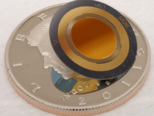
The Sources and Detectors Group conducts research on the characterization of lasers, detectors, and related components. Principally through measurement services and innovation, the group provides the optoelectronics industry with traceability to national standards. Activities of the group are currently carried out in three project areas: Laser Radiometry, Laser Applications, and Terahertz Imaging and Sources. Examples of some of these devices fabricated in the BMF include: Superconducting Planar Nanotube Radiometers, Absolute Radiometers for Space Research, and SmartMirrors for laser-based manufacturing.
The Lehnert Group develops quantum coherent interfaces that allow the transfer of information between superconducting qubits, propagating light fields, and trapped ion qubits, to enable the development of quantum networks and distributed quantum information processors. Most of the groups devices are manufactured in the BMF.
The Faint Photonics Group develops new light sources, detectors, and measurement techniques that operate at the few photon limit to address national needs in the areas of quantum information science, remote sensing, long-distance communications, and imaging. The smallest unit of light is a "photon". Generation, manipulation and measurement of light at or near the fundamental limit of a photon can enhance the performance of many optical systems. Remote sensing, long-distance communications, biological imaging, and quantum information science are some near-term applications that would benefit immensely from better optical components and techniques that work efficiently at few or single photon levels. However, the technologies to generate, manipulate, and detect these states of light are inadequate for the emerging applications. The single photonics and quantum information project staff develops new light sources, detectors, and measurement techniques to address these needs. The group uses the BMF to fabricate their detectors and waveguides.
The Quantum Nanophotonics Group develops and provides advanced measurement technology, methodology, and test structures to support the efficient manufacture and characterization of optoelectronic components. The Group also develops new photonic devices in support of NIST and other government programs. Two major focus areas are compound semiconductor nanotechnology and quantum information. The group uses the BMF to fabricate their semiconductor devices and waveguides.
The Magnetic Imaging Group develops calibration methods, standards, and contrast agents for magnetic imaging technologies as needed by the U.S. healthcare industry and the U.S. government to advance and validate quantitative biomagnetic imaging methods. The group has used the BMF to fabricate their magnetic devices and their RF contrast agents.
Quantum Processing Group
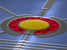
The Quantum Processing Group develops new technologies for processing information using superconducting circuits. In addition, they develop advanced fabrication techniques are to enable true scaling of both superconducting quantum computers and ion-trap based systems. Examples of devices include parametric amplifiers and frequency combs based on superconductors with high kinetic inductance and new geometries for superconducting quantum binary devices as fundamental building blocks for quantum computing. The group uses the BMF to fabricate devices.
Even if the power needs for all U.S. data centers can be met, the inherent constraints of semiconductor electronics will still impose scaling and clock-rate limits on future processing capacity at a time when the digital information is increasing exponentially. Electron-spin torque may be used to switch future, nonvolatile, magnetic memory elements. Compared to switching memory bits with magnetic fields, this method would offer higher speed, greater reliability, lower power, and would be scalable to smaller device dimensions. The Spin Electronics Group investigates theoretical and experimental aspects of spin transport and the transfer of spin angular momentum to magnetic structures. The Spin Electronics Group uses the BMF to fabricate their devices.
Nanoscale Spin Dynamics Group
The Nanoscale Spin Dynamics Group develops new measurement techniques to characterize the high frequency properties and performance of nanomagnetic structures and devices. Hard-disk drives in personal computers and data centers push the limits of technology, with current data bit densities of 100 billion per square centimeter. The controlled switching of magnetization in write heads, read heads, recording media, and innovative memory elements at frequencies in the hundreds of megahertz to hundreds of gigahertz will be the foundation for future magnetic data storage systems and advanced microwave integrated circuits. These technologies will depend on newly discovered properties and limitations of magnetic materials and devices that appear only at the nanoscale. The Nanoscale Spin Dynamics Group uses the BMF to fabricate their devices.
Quantum Sensors Group
The Quantum Sensors Group, part of NIST’s Physical Measurement Laboratory, and the Quantum Electromagnetics Division, advances the detection of photons and particles in a variety of application areas using superconducting sensors and readout electronics. Major group activities include: superconducting x-ray and gamma-ray spectrometers for applications that include materials analysis and nuclear materials accounting, superconducting microbolometers for applications that include concealed weapons detection and understanding the early universe, advanced cryogenics to aid the dissemination of cryogenic sensors, the determination of x-ray fundamental parameters to facilitate materials analysis by x-ray techniques, and support of U.S. industries that develop or use advanced cryogenics and cryogenic sensors. The Quantum Sensors Group uses the BMF to fabricate their devices.

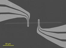
The Ion Storage Group conducts experiments on atomic ions that are confined in electromagnetic traps and laser-cooled, in some cases, to the ground state of motion. Experiments employ RF (Paul) traps and Penning traps. In one area of research the groups uses trapped ions to control quantum-mechanical systems. This research can potentially revolutionize technologies including computing, simulation, secure communication and precision metrology. A second area of research focuses on the use of trapped ions for precision measurements. In particular, they are interested in optical frequency metrology, which provides the basis for diverse applications from optical clocks to tests of fundamental physics and relativistic geodesy. The Ion Storage group uses the BMF to fabricate ion traps.