
Official websites use .gov
A .gov website belongs to an official government organization in the United States.
Secure .gov websites use HTTPS
A lock (
) or https:// means you’ve safely connected to the .gov website. Share sensitive information only on official, secure websites.
Flux Quantum Electronics
Description
Superconductive Circuits for Cryogenic Quantum Computing
Quantum computing, and in particular cryogenic superconducting quantum computing with its demonstration of “Quantum Supremacy”, has made tremendous progress over the past decade with many US companies playing primary roles in this revolutionary development. However, building quantum computers powerful enough to solve useful problems will require thousands if not millions of physical quantum bits (qubits), and this scaling problem presents some substantial technological hurdles. One such hurdle is a scalable and low-latency solution for qubit control and readout electronics, avoiding the “rat’s nest” of wires and cables connecting the racks of room temperature electronics to the qubits in the cryostat.
The NIST FQE research team is investigating superconductive microwave and mixed-signal circuits for the control and readout of cryogenic quantum bits (qubits) in a quantum computer. This work is in collaboration with multiple NIST groups and is funded by NIST in support of the National Quantum Initiative Act and the White House National Strategic Overview for Quantum Information Science. We are also collaborating with universities and the Department of Energy’s SQMS center in distinct but related work. The goal of this work is to assist US industry in their efforts to develop fault-tolerant quantum computers.
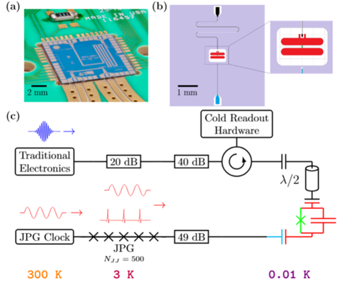
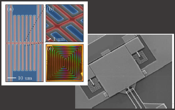
In 2022, the NIST team demonstrated that they could initialize and control the state of a superconductive qubit using digital pulses from superconductive circuits using NIST’s JAWS technology from the Quantum Voltage Project. In 2023, the team improved on this work and demonstrated single qubit gate fidelities greater than 99.5%, limited by the coherence of the qubit. (See Fig. 1.). Also in 2023, NIST collaborated with two distinguished university teams to demonstrate qubit control using pulses from a single-flux-quantum (SFQ) circuit, with the classical SFQ control chip and the qubit chip combined in a multi-chip module. The FQE team continues to investigate the fundamental limits to qubit control using this technology and is also pursuing scalable readout solutions using SFQ-based electronics.
RF calibrations for Quantum Computing
The FQE team is participating in a multi-laboratory project described here: Getting from Qubit to Mega-Qubit Quantum Computers with Radio Frequency (RF) Calibrations. In this collaboration, we have developed an ultra-sensitive power sensor as part of a NIST custom cryogenic front-end for a vector network analyzer. Also as part of this multi-laboratory RF calibrations project, the FQE team is collaborating with Google and Menlo Micro to develop radio frequency cryogenic switch networks as a critical enabling technology for quantum information science for both calibration and high throughput testing of samples. Note: collaborations do not indicate endorsements of tested technologies.

Power Sensor and Single Photon Generator: We are developing a device consisting of a superconducting transmon qubit device that is strongly coupled to a transmission line for use in several quantum technology applications and for calibration purposes of dilution refrigerators used for quantum computing experiments. The FQE team has demonstrated that this device can be used as an absolute power sensor with a sensitivity down to -150 dBm (1 attowatt!) for calibrating and characterizing transmission line attenuation (see Fig. 2), microwave components, or other devices inside the dilution refrigerator. Since the transmon qubit device can be approximated as a two-level system, it absorbs and emits only single microwave photons, making it an on-demand microwave single-photon source. To demonstrate the quantum nature of the emission state, we reconstructed its Wigner function and measured the second-order correlation function. This work was recently submitted for publication.
Cryogenic Microwave Switch Networks: Traditionally, electromechanical switches have been used for cryogenic switch matrices but our approach is to use MEMS-based (Micro Electro Mechanical Systems) switches due to their lower power dissipation and smaller size, and to minimize the risk that solenoid switches tend to produce current pulses that destroy expensive cryogenic amplifiers and can cause electrostatic damage to devices. We are developing a cryogenic-compatible, open-sourced solution that includes all design files, software, and other necessary documents for 1) building a PCBA-based switch network, and 2) a room temperature control system that provides direct control of the switches in a 19-inch rack-mount package.
Hot Qubits
Superconducting qubits operating at frequencies between 1 GHz and 10 GHz are one of the leading candidates for implementing quantum information systems. These qubit circuits have led to laboratory proof-of-principle demonstrations of quantum computing with ~100 qubits and to a nascent commercial quantum industry. However, operation is limited to very cold temperatures (<0.05 K), severely limiting the scalability and commercial viability of this technology. The FQE team is leading an internal collaboration that includes researchers from two NIST campuses as well as NIST scientists at Brookhaven National Laboratory to develop the measurement science needed to extend superconducting qubit operating frequencies to the 10 GHz to 100 GHz range. This higher frequency paradigm using “hot qubits” requires concurrent research efforts in quantum materials science, single-photon detection metrology, and qubit device metrology.
In exploring this new paradigm, NIST is developing new measurement technologies and capabilities in the (10-100) GHz band that are likely to foster much broader metrology applications in quantum information, quantum sensing, quantum networking, and wireless communications.
Credit:
CTL
|
Credit:
CTL
|
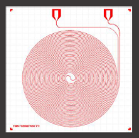
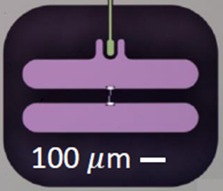
| Fig. 4. The Hot Qubit project is also developing, in collaboration with Prof. Taylor Barton at the University of Colorado, superconducting microwave frequency multipliers using the nonlinearity and large kinetic inductance of niobium-titanium-nitride (NbTiN). Shown on the left is a spiral coplanar waveguide transmission line multiplier on a 1-cm square chip. This device is used to generate higher frequency harmonics (up-conversion) in situ for control and readout of high frequency qubits while avoiding high-frequency attenuation that would occur if the signals were transmitted from outside the cryostat. On the right is an image of a superconducting qubit, showing the large (pink) niobium capacitor pads connected by a thin aluminum line (white) with a Josephson junction. | |
Credit:
CTL
|
Credit:
CTL
|
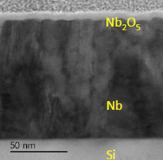
| Fig. 3. The NIST “Hot Qubit” project includes identifying and quantifying sources of device performance loss in the (10-100) GHz frequency range and correlating that loss to chemical and physical materials analysis. Shown on the left is a cross-sectional image from a scanning tunneling microscope of a niobium (Nb) film grown on a bare silicon wafer. To measure qubit devices in this frequency range, NIST is developing new parametric amplifiers. Shown in the center and right are scanning electron microscope images of parametric amplifiers fabricated in the NIST Boulder Microfabrication Facility. | |
Superconductive Advanced Computing
Processor speed, power dissipation, and energy use, especially in this era of Artificial Intelligence technologies, are major challenges for US industry in advancing computing systems from cell phones to large-scale supercomputer systems. Superconducting computing, using single-flux-quantum (SFQ) cryogenic circuits with Josephson junctions as switches that produce small current pulses and superconducting interconnects to transmit those pulses as the digital “bits”, dissipate extremely little power, can operate at clock rates well above 100 GHz, and are potentially competitive for certain applications on the basis of power and energy efficiency if key component technology issues can solved.
NIST is developing niobium-based superconductive devices, materials, fabrication processes, and cryogenic electrical measurements to support energy-efficient, high-speed, superconductive digital computing through the government’s FSDL program. Using the Boulder Microfabrication Facility and working with the Quantum Voltage team, our team is developing processes for fabricating SFQ-based circuits with large numbers of Josephson junctions (JJs) that operate at faster speeds and with higher yields. Fig. 5 shows a cross-sectional image, generated by NIST’s scanning electron microscope with focused ion-beam (FIB-SEM) capability, of the layer stackup from a wafer fabricated using the NIST SFQ process on a 3” silicon substrate. It features four niobium (Nb) metal layers (M0-M3), a bias resistor layer (RS), and Josephson junctions (JJs). The first two metal layers are fully planarized using chemical-mechanical polishing (CMP).
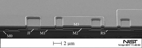
Fig. 5. Scanning electron micrograph of a superconducting integrated circuit fabricated at NIST. The chip has been cross-sectioned using a focused ion-beam to show the multi-layer micro-fabrication we use to produce flux quantum electronics. The layers identified are the superconducting niobium metal layers (M0-M3) and Josephson junction (JJ), and the non-superconducting bias resistor layer (RS).
Fig. 6 shows a digital circuit fabricated and measured at NIST which operated up to 300 GHz (Fig. 6).
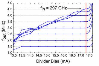
Fig. 6. Plot of measured output frequency at T = 4 K of a 16-stage static divider based on a design provided by an US industrial collaborator. Each curve corresponds to a fixed input frequency. The flat sections indicate the operating margin. The top-most curve shows a maximum operating frequency of 297 GHz.
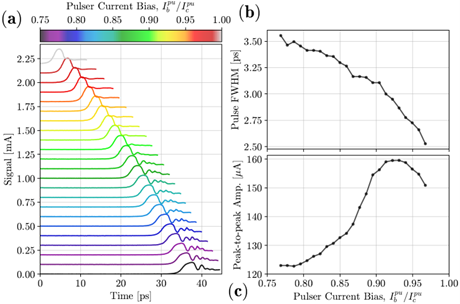
Josephson Sampler: The FQE team is also developing Josephson sampler technology to support energy-efficient, high-speed, superconductive digital computing through the Department of Defense FSDL program. Our goal is to provide a circuit diagnostic tool that performs as a sampling oscilloscope but operates at cryogenic temperatures and with extremely high bandwidth. This tool could be used to measure signals in digital superconductive electronics to assist in circuit design, model-to-hardware correlation, verification of circuit performance, and failure analysis.
Measurement of signals generated by superconducting Josephson junction (JJ) circuits require ultrafast components located close to the generating circuitry. Recently, the FQE teams has designed, simulated, fabricated, and tested a sampler with electrical bandwidth exceeding 100 GHz to measure ultra-fast electrical signals generated from superconducting analog and digital circuits. (See Fig. 7.) This work has been submitted for publication to the Review of Scientific Instruments, titled “Picosecond Josephson Samplers: Modeling and Measurements.”
RF Reference Sources for Wireless Communications
The demand for wireless communications has exploded over the last 2 decades and there is no end in sight. The quest for higher bandwidth is driving the use of higher carrier frequencies in the microwave and millimeter-wave (>30 GHz) bands. However, there are no primary reference signal standards at these frequencies. What is used now is a receiver that measures the power of an incoming signal (e.g. a thermal voltage converter). A reference source at 5G wireless frequencies would be a game-changer, enabling faster deployment of new wired and wireless technologies.
To fulfill this need, the FQE team is developing quantum-based reference sources, programmable waveform synthesizers, and even comb generators for these frequencies. We are building on the success of NIST’s programmable Josephson Arbitrary Waveform Synthesizer (JAWS), the NIST Standard Reference Instrument for ac voltage (up to audio frequencies), and are exploring new ways to develop superconductor-based, higher-speed, accurate AWS sources for use as calibration standards. Recently, the FQE team together with the Quantum Voltage team has demonstrated several high-speed modifications to the JAWS design capable of reaching frequencies above 5 GHz. Together with the Communications Technology Laboratory, the team is developing the theory and techniques to transfer the on-wafer quantum-based accuracy to room temperature and has published calibrated measurements of the output power of these circuits for synthesized signals up to 1 GHz.
This demonstration at 1 GHz is an improvement of 100,000 times in frequency over the existing audio frequency JAWS. However, it is not fast enough to serve as a calibration tool for the full range of 5G signal frequencies. To make reference sources for these higher frequencies, FQE researchers are employing “single flux quantum” (SFQ) technology. Extremely tiny, brief, and accurate electrical output pulses are emitted from Josephson junctions when they are excited by an electrical signal. Like many properties at extremely small scales, these tiny electrical pulses are quantized – that is, they can only take on exact, discrete values, the smallest possible amount of which is a single flux quantum. And because they are quantized, their values are precisely known and equal to the ratio of two fundamental constants of nature, the key to making a reference standard.
In 2018, a conceptual design for an SFQ-based “Synthesizer-on-a-Chip” (SOC) was proposed by the FQE team. In a 2021 publication, first authored by Manuel Castellanos-Beltran, key sub-circuits of that SOC have been demonstrated. Fig. 8 shows a power spectrum of a 4 GHz signal synthesized by the 8-fold voltage multiplier circuit shown in Fig. 9.
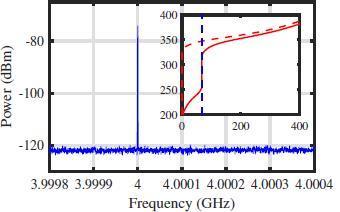
Fig. 8 - Power spectrum output of a 4 GHz sine wave synthesized with the x8 voltage multiplier circuit shown in Fig. 9. Inset: red dc current-voltage (I‑V) curve (y-axis in microamperes, x-axis in microvolts) showing the expected constant voltage step (dashed-blue line) associated with the digital code sent to the chip. Dashed-red curve is the I-V curve when no pulses are sent.
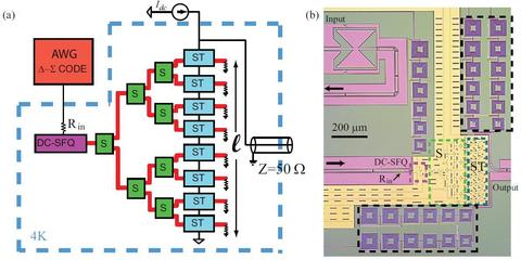
Fig. 9. (a) Simplified schematic of the x8 voltage multiplier (VM) device under test (DUT) described in this report. (b) Picture of a portion of the fabricated DUT chip. The DC-SFQ converter and the splitter (S) and SQUID transformer (ST) network appear in yellow and are labeled. The purple spiral inductors enclosed in the black-dashed boxes are used as low-pass filters for bias lines of the device and to perform the DC measurements, i.e. current voltage characteristics and quantum-locking ranges. At both the input (left) and the output (right) of the VM, the signal is launched into the pink coplanar waveguide transmission lines.
This work also supports Congress’ directive to NIST for advancing microelectronics technology and specifically for developing measurements and tools for ensuring secure, tamper-proof wireless communication systems. The FQE team is collaborating with researchers in NIST’s Communications Technology Laboratory, who are investigating “over-the-air” identification techniques, i.e. analyzing transmitted electromagnetic signals from wireless equipment and systems, to identify potential threats for secure communications. This work would benefit from a reference source that can provide a “clean” (free of noise and distortion) signal for calibrating their test equipment.
Major Accomplishments
M. A. Castellanos-Beltran et al., "Measurable Improvement in Multi-Qubit Readout Using a Kinetic Inductance Traveling Wave Parametric Amplifier," in IEEE Transactions on Applied Superconductivity, vol. 35, no. 5, pp. 1-5, Aug. 2025, Art no. 1500305, doi: 10.1109/TASC.2024.3525451.
M. A. Castellanos-Beltran, A. J. Sirois, L. Howe, D. Olaya, J. Biesecker, S. P. Benz, P. F. Hopkins, “Coherence-limited digital control of a superconducting qubit using a Josephson pulse generator at 3 K,” Appl. Phys. Lett. 8 May 2023; 122 (19): 192602. doi: 10.1063/5.0147692
L. Howe, B. van Zeghbroeck, D. Olaya, J. Biesecker, C. J. Burroughs, S. P. Benz and P.F. Hopkins, “Picosecond Josephson Samplers: Modeling and Measurements,” arXiv:2503.20022 [physics.ins-det], 25 Mar 2025.
C. A. Donnelly, N. E. Flowers-Jacobs, J. A. Brevik, A. E. Fox, P. D. Dresselhaus, P. F. Hopkins, S. P. Benz, "1 GHz Waveform Synthesis With Josephson Junction Arrays," IEEE Trans. Appl. Supercond., vol. 30, 1400111, 3 April 2020, doi: 10.1109/TASC.2019.2932342.