

Official websites use .gov
A .gov website belongs to an official government organization in the United States.

Secure .gov websites use HTTPS
A lock (
) or https:// means you’ve safely connected to the .gov website. Share sensitive information only on official, secure websites.


GlobalWafers (Texas)
Key Facts
Project Summary
The U.S. Department of Commerce made direct funding awards to GlobalWafers America, LLC (GWA) and MEMC LLC (MEMC), subsidiaries of GlobalWafers Co., Ltd. (GlobalWafers), of up to $406 million to support the construction of new wafer manufacturing facilities in Sherman, Texas and St. Peters, Missouri.
Economic and National Security Impact
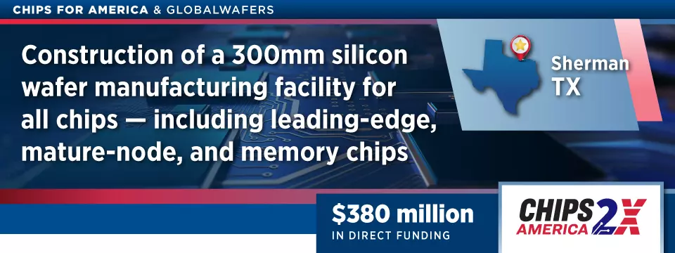
Silicon wafers, which will be produced by GWA in Sherman, Texas, are foundational components in the semiconductor ecosystems, serving as essential inputs for all chips, including leading-edge, mature-node, and memory chips. Approximately 90% of silicon wafers are sourced from East Asia today, with five corporations managing the majority of global supply – GlobalWafers is one of the five global leaders in this market. Accordingly, by supporting this facility, the U.S. is taking a meaningful step to strengthen supply chain resilience and help support a reliable domestic supply of key semiconductor components.
Silicon-on-Insulator (SOI) wafers, which will be produced by MEMC in St. Peters, Missouri, are critical for advanced semiconductor applications as they enable higher performance, lower power consumption, and improved thermal efficiency, making them essential for cutting-edge technologies in defense, aerospace, and high-performance computing. SOI wafers can also be made to feature radiation-hardened characteristics, which are critical for semiconductor performance and reliability for several defense and aerospace end uses. This project will serve as the key domestic site for 300mm SOI wafers in the U.S., helping to advance U.S. economic and national security by significantly expanding domestic capacity and technological capabilities.
Finally, as part of the award agreement, GlobalWafers has agreed to convert a portion of its existing silicon epitaxy wafer manufacturing facility in Sherman, Texas to silicon carbide (SiC) epitaxy wafer manufacturing, producing 150mm and 200mm SiC epitaxy wafers. SiC epitaxy wafers are a critical component for high-voltage applications, notably including electric vehicles and clean energy infrastructure.
GlobalWafers Project Overview | ||
|---|---|---|
Project Summary | Recipient | GlobalWafers |
| Location(s) | Sherman, Texas St. Peters, Missouri | |
Financial Summary | Program | CHIPS Program Office |
| Direct Funding Amount | Up to $406 million | |
| Expected Capital Expenditure | $4 billion | |
Workforce Summary | Estimated Job Creation | Approximately 1,700 construction jobs and 880 manufacturing jobs across Texas and Missouri |
| CHIPS Workforce Funding | $6 million | |
Project Statistics: Sherman, Texas | ||
|---|---|---|
Summary | Project Type | Construction of a 300mm silicon wafer manufacturing facility |
| Estimated Job Creation | Approximately 1200 construction jobs 750 manufacturing jobs | |
| Direct Funding | $380 million | |