U.S. flag

An official website of the United States government

Official websites use .gov
A .gov website belongs to an official government organization in the United States.

Secure .gov websites use HTTPS
A lock ( ) or https:// means you’ve safely connected to the .gov website. Share sensitive information only on official, secure websites.

Projects/Programs

Displaying 26 - 50 of 112

Electronic Material Characterization

Ongoing
Manufacturing optimized devices that incorporate newly-emerging materials requires predictable performance throughout device lifetimes. Unexpected degradation in device performance, sometimes leading to failure, is often traceable to poor material reliability. Reliability is rooted in the stability...

Electronics for Cryogenic Environments

Ongoing
The operation of electronics optimized for room temperature applications in cryogenic environments introduces a remarkable number of physical and engineering hurdles. It is unsurprising that devices and circuits designed for room temperature encounter shifts in their operation parameters in...

Electron-Solid Interactions

Ongoing
A measuring instrument produces a signal that depends upon the value of the measurand. The value and its uncertainty are inferred from the signal by using a model of their relationship. Erroneous models lead to erroneous inference. The accuracy of SEM (scanning electron microscopy) is limited by...

Emerging Power Electronic Devices

Ongoing
The ongoing electrification of society has elevated the importance of electric transportation, renewable energy distribution, and data centers. It has also put new demands on the technologies -- called power electronics -- that control, interface, and transmit the electrical energy that powers our...

Enriched Silicon and Devices for Quantum Information

Ongoing
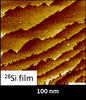
Enriching silicon from 5% to <1 ppm 29Si Groundbreaking work around the world has realized qubits in silicon using metal-oxide-semiconductor (MOS) devices, single atomic dopants/defects and SiGe heterostructures, and, in all cases, the qubit coherence and fidelity properties are improved when using...

EUV Scatterometry

Ongoing
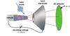
To measure and inspect the smallest printed features on an IC chip, researchers and manufacturers use a combination of electron scanning modalities (i.e., transmission electron and scanning electron microscopies) and an optical method, scatterometry. Industrially, the most common modality for...

Evaluation of 2D and WBG Material Quality Toward Device Reliability

Ongoing
Two-dimensional (2D) and wide band gap (WBG) materials are some of the latest materials classes having the potential to be transformative because of their high carrier mobilities, tunable bandgap, and atomic-scale film thicknesses. Unexpected degradation and failure in device performance is often...

Extreme Atom Probe Tomography

Ongoing
Sub-nanometer-resolved 3-D chemical mapping of any atom in any solid continues to be an imperative goal of materials research. If reduced to practice, it would have profound scientific, engineering, and economic impacts on U.S. industries collectively worth hundreds of billions of dollars. Such...

Extreme ultraviolet optical constants

Ongoing
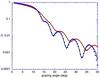
Measurements of EUV optical constants are often made by measuring the absorption or near-normal-incidence reflectivity, then performing transforms to obtain both the real and imaginary parts of the index. These sorts of measurements have considerable uncertainty because they require knowledge of...

Fundamental Electromagnetic Technologies and Standards

Ongoing
This focus area develops theory, metrology, and standards for the technologies upon which the future of both wired and wireless communications depends. These developments are then leveraged to provide better measurement services to U.S. industry through extended frequency range, lowered uncertainty...

Fundamental Metrology for Communications

Ongoing
Engineers designing the next generation of wireless applications and devices must work around the fundamental issue of radio interference. NIST CTL’s RF Technology High Speed Electronics group focuses on fundamental measurement and modeling of nonlinear microwave systems, devices and materials that...

GaN Nanowire Growth

Ongoing
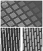
Selective epitaxy: We have demonstrated that the diameter and placement of nanowires can be controlled by using silicon nitride (SiNx) masks on top of MBE-grown buffer layers (see figure). With electron beam lithography, several patterns with 3 mm die size that provide over 100,000 controlled...

GaN Nanowire Metrology and Applications

Ongoing
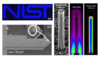
GaN Nanowire LEDs: Our selective epitaxy methods and dopant characterization techniques have enabled fabrication of arrays of nanowire LEDs with controlled location and spatial layout. This development is complemented by modeling of the carrier flow and recombination. These LEDs were combined to...

Genomics of Electronic Materials

Ongoing
We approach this multidimensional characterization problem by developing measurement-based techniques to rapidly quantify all of the relevant properties of thin-film materials, interfaces, and microelectronic structures. We make extensive use of finite-element simulations, as well as linear and non...

Hardware Accelerators for Neural Networks

Ongoing
One promising candidate for building a hardware accelerator comes from the field of spintronics, where information is carried by electronic spin rather than charge. Magnetic tunnel junctions are particularly suited because of their multifunctionality and compatibility with standard integrated...

Hardware Accelerators for Statistical Computing

Ongoing
Finding good solutions to many hard problems, like combinatorial optimization and traveling salesman problems, counterintuitively requires making the estimated solution worse before making it better. This situation results from many hard problems having many “solutions” that cannot be improved...

High Speed Metrology for Magnetoelectronic Devices and Models

Ongoing
The U.S. Semiconductor industry is integrating ferromagnet-based microelectronic devices such as magnetic RAM (MRAM) into existing silicon-based technologies. MRAM has much shorter write times and higher write endurance than the embedded Flash currently used. These properties makes MRAM highly...

High Temperature Hall Effect Measurements

Ongoing
Customized Hall effect measurement apparatus which supports measures of Hall effect mobility and resistivity of semiconducting films across a wide range of temperatures (77K-825K).
Was this page helpful?