
Official websites use .gov
A .gov website belongs to an official government organization in the United States.
Secure .gov websites use HTTPS
A lock (
) or https:// means you’ve safely connected to the .gov website. Share sensitive information only on official, secure websites.
Summary
The state of the art for measurement and inspection of the smallest printed features on an integrated circuits (IC) chip is a combination of electron scanning modalities and an optical method, scatterometry. Scatterometry provides the industry with quantitative information through modeling and inverse regression about average feature sizes over millions of devices at a time.
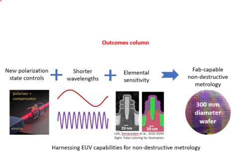
This project will use scatterometry to benefit advanced IC manufacturing by developing novel extreme ultraviolet (EUV) optics, tabletop sources, and methodologies for inspection and process control.
Grand Challenge 2. Advanced Metrology for Future Microelectronics Manufacturing
Description
To measure and inspect the smallest printed features on an IC chip, researchers and manufacturers use a combination of electron scanning modalities (i.e., transmission electron and scanning electron microscopies) and an optical method, scatterometry.
Industrially, the most common modality for scatterometry is spectroscopic ellipsometry (SE), where changes in the polarization state of light reflected from the structures are analyzed as a function of wavelength. Utilizing near-infrared, visible, and deep-ultraviolet wavelengths, scatterometry is fast, non-destructive, and relatively inexpensive compared to electron-scanning methods.
It is currently difficult to characterize sub-10 nm wide semiconductor patterns with scatterometry, and the measurement challenge grows significantly as new materials and strain engineering are incorporated into complex nanometer-scale 3-D device geometries.
The industry needs innovations in scatterometry to measure beyond visible and ultraviolet wavelengths, and into the spectral region from 10 nm to 150 nm to measure future semiconductor devices. Through a combination of ten times greater spatial resolution in each dimension and the ability to penetrate materials using shorter wavelengths, this project will achieve an increase in the information gathered through fast optical techniques by a factor of 1000 and will transfer these technologies to U.S. semiconductor industry.