Summary
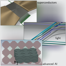
Artificial intelligence increasingly affects many aspects of society. New computational hardware based on information-processing in the brain is being developed to lead to more powerful AI systems. Working within this field of “neuromorphic computing”, our project combines integrated photonics for communication with superconducting electronics for computation to construct large-scale neuromorphic systems for AI. Optical signals broadcast over a network of nanophotonic waveguides enable massive connectivity between artificial neurons. Superconducting single-photon detectors integrated with waveguides enable communication at the physical limit of energy efficiency. Superconducting electronic circuits based on Josephson junctions are excellent for performing neural computations. Together, synapses, dendrites, and neurons combining these devices can achieve the complexity, connectivity, and scale of the human brain. We are developing the devices and systems to realize superconducting optoelectronic networks for neuromorphic supercomputing.
Description
Our work in this area can be separated into two categories: conceptual and experimental. Please read our publications linked below for more information.
Experimental:

Our latest generation of synaptic circuits are described in a 2024 paper published in APL Machine Learning. These circuits are our first demonstration of synapses with an integrated local memory that can be programmed to define a synaptic weight. The memory element is a simple superconducting loop, whose state can be changed at the level of individual quanta of magnetic flux. This memory has many attractive properties including extremely high endurance, low programming energies, high programming speeds, long retention times, hundreds of available states, and compatibility with our single-photon sensitive synapses. Such local plastic memories are key to eliminating the von-Neumann bottleneck and developing neuromorphic systems with fully parallel on-chip learning.

We demonstrated superconducting pixels for a novel class of highly scalable single-photon sensitive cameras. Published in 2024, this work introduced on-chip circuits made from Josephson junctions that locally count and store detection events from superconducting nanowire single-photon detectors. This class of detector boasts state-of-the-art performance in many metrics, but applications have been limited by the inability of readout architectures to keep up with the rate of photon detection in large-scale arrays. Our approach makes such arrays compatible with conventional CMOS readout architectures, significantly increasing the rate at which individual photons can be counted. This could have a major impact on a variety of fields including integrated circuit evaluation and failure analysis, astronomical observation, and biomedical imaging.
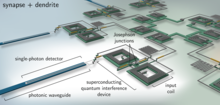
In 2022, we demonstrated the first superconducting optoelectronic synapses and published the work in Nature Electronics. These synapses performed weighting and leaky integration of single-photon presynaptic signals and showcased behavior very similar to their biological counterparts. Leak rates spanning four orders of magnitude (250 ns - 6 ms) were demonstrated, suggesting that SOENs can be a powerful information processing system across many different timescales and applications. The work also established the feasibility of monolithically integrating superconducting nanowire single-photon detectors with Josephson junctions, setting the stage for large-scale manufacturing of the technology.

In a paper in Physical Review Applied published in 2020, we presented progress toward large-scale arrays of single-photon detectors for artificial synapses. Such hardware innovations may contribute to neuromorphic systems with energy-efficient, light-speed photonic communication across densely connected spiking neural networks.
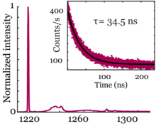
Also in 2020 we presented silicon light sources one-hundred times brighter than our previous work. This work also demonstrates the production of these emissive centers at the scale of 300-mm wafers, a technology enabled by our collaboration with SUNY Polytechnic Institute. Continued progress in this area may lead to silicon light sources capable of meeting all the demands for communication large-scale spiking neural networks, thereby presenting a promising path toward scalable neuromorphic hardware with dense network communication and low manufacturing cost.
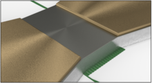
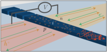
An ultrahigh impedance superconducting thermal switch for interfacing superconductors with semiconductors and optoelectronics demonstrates a superconducting voltage amplifier enabling a mV superconducting signal to drive a semiconductor diode at 1V to generate light. This component is central to the ability to achieve superconducting optoelectronic neurons. The work was published in Nature Electronics.
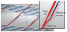
Design, fabrication and metrology of 10x100 multi-planar integrated photonic routing manifolds for neural networks is a recent implementation of a feed-forward routing architecture with all-to-all connectivity using two photonic planes.
Multi-planar amorphous silicon photonics with compact interplanar couplers, cross talk mitigation, and low crossing loss is our first demonstration of multi-planar waveguide interconnects. We show three planes of amorphous silicon waveguides with low-loss inter-planar couplers and crossings.

All-silicon light-emitting diodes waveguide-integrated with superconducting single-photon detectors demonstrates electrically injected light sources waveguide-coupled to superconducting single-photon detectors. These are two primary components of superconducting optoelectronic neurons.
Room-temperature-deposited dielectrics and superconductors for integrated photonics presents related integrated photonic demonstrations from our group at NIST.
Conceptual:
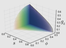
We have developed a new simulation framework for superconducting optoelectronic networks, described in a 2023 publication in Physical Review Research. Previous simulations modeled every device (single-photon detector, Josephson junction, etc.) from first principles which is computationally slow and only practical for small circuits. We developed a phenomenological model that increases simulation speeds by a factor of ten thousand, while maintaining close agreement with the brute force approach. This has since evolved into a high-level simulation codebase for modelling full networks and experimenting with neuromorphic algorithms. This software is publicly available at https://github.com/ryangitsit/sim_soens.
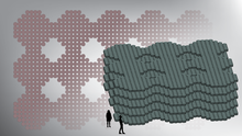
The goal of this project is to pursue optoelectronic intelligence. This perspective article summarizes the motivations for the project, the physical requirements for attaining intelligent systems, and the hardware considerations that lead us to pursue integration of optical components for communication with superconducting electronics for computation to enable large-scale neural systems.
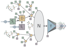
Fluxonic processing of photonic synapse events explores the use of simple SNSPD/JJ circuits that perform many functions associated with synaptic and dendritic computation in neural systems.
Circuit designs for superconducting optoelectronic loop neurons is a recent paper we wrote for the JAP special issue on new physics and materials for neural systems. It is the quickest summary of loop neurons circuit concepts.
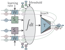
Superconducting optoelectronic loop neurons is a more thorough treatment of the circuits and systems summarized in the above paper.
Design of superconducting optoelectronic networks for neuromorphic computing was presented at IEEE Rebooting Computing 2018. This work utilized the evolutionary optimization software developed by TennLabs in conjunction with a model of superconducting optoelectronic neurons to design networks capable of solving the TennLabs benchmark problems.
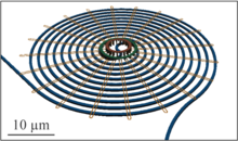
Superconducting Optoelectronic Circuits for Neuromorphic Computing is our first paper on the subject. It represents our early thinking.
Opportunities:
We currently have opportunities for postdocs. NIST Boulder and the University of Colorado are within walking distance of each other, creating a vibrant intellectual and scientific community. With over 300 sunny days per year and ample opportunities for outdoor and cultural recreation, Boulder is an excellent place to live. The salary of a starting postdoc at NIST is $70,000, far superior to many academic postdoc salaries. Please contact Jeff Shainline (jeffrey.shainline [at] nist.gov (jeffrey[dot]shainline[at]nist[dot]gov)) if you are interested in these opportunities.

