
Official websites use .gov
A .gov website belongs to an official government organization in the United States.
Secure .gov websites use HTTPS
A lock (
) or https:// means you’ve safely connected to the .gov website. Share sensitive information only on official, secure websites.
Electronic and Chemical Properties of Systems for Advancing Solid State Quantum-based Devices
Summary
The electronic properties of a material govern how they will be used in device form. We apply electron-based analytical methods to image the electronic properties and measure energy levels of candidate materials in electronic systems which will provide insight on how to integrate these systems in device form. We also alter and engineer heterostructures to implement and harness novel properties in these systems, in order to move beyond materials discovery to engineered properties to guide further development of these technologies.
Description
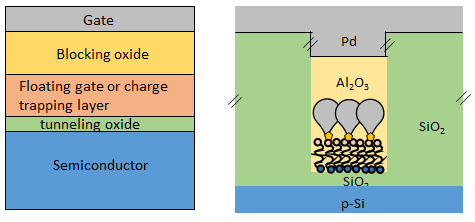
Schematic cross-sectional drawing (not to scale) of a prototypical Flash-based memory device (left) and the molecular memory device in a capacitor structure (right).
Development of new electronic devices for specific functionality and applications typically involves integrating new semiconducting materials. The electronic band structure of a solid is a fundamental property which defines how a material will be used and integrated into device form. Electronic properties and energy levels are not universal values for a given system. For a single crystalline material, the work function value varies with crystallographic planes. In less mature technologies where fabrication quality is still in development, this becomes very apparent on the dependency of electronic/optical and structural properties on the growth and device fabrication methods. One of the most common ways to probe the electronic structure (e.g., band structure) is by way of photoemission (PES or photoelectron spectroscopy). We apply electron-based analytical methods to directly access the electronic and chemical properties of novel electronic materials.
We apply a suite of advanced electron-based measurement methods to measure and characterize electronic properties such as one photon photoelectron spectroscopy (XPS, UPS), inverse photoemission (IPES), and photoemission electron microscopy (PEEM). NIST Gaithersburg is home to a unique suite of electron spectroscopy, with capability spanning both occupied and unoccupied density of states (DOS) and analytical lateral area from 100 μm2 (PEEM), 1 mm2 (UPS/XPS), to 1 cm2 (IPES). We also collaborate with the Helmholtz Zentrum Berlin for measurements using a novel, angle-resolved time-of-flight (ARTOF) electron spectrometer which allows for efficient access to the valence band for “small” and radiation-sensitive systems. We work in close collaboration with materials growers and synthesis, device physicists, and electrical engineers to probe relevant interfaces to advance nanoscale electronic technologies.
Memory devices incorporating molecular layers. In the era of hyperscaling of traditional semiconductor transistors, this requires other system components such as non-volatile memory to follow similar trends. A hybrid NAND FLASH memory device utilizing a molecular layer to assist in charge trapping is a possible candidate for enabling dimensional scaling.
Novel Electronic Materials and Systems. Non-silicon semiconducting channel materials are considered for flexible electronic applications, quantum devices, and power electronics. Some of these candidates include carbon- and molecular-based semiconductors, atomically-thin van der Waals materials, and wide bandgap semiconductors. With these new systems, we must adapt our metrology techniques in order to accurately measure electronic and chemical properties such as by laser-assisted PES.
Major Accomplishments
2021
Begin projects on investigating on the electronic and electrical properties of pn GaN and b-Ga2O3 for advancing power electronics
2020 - 2021
Commissioning of inverse photoemission (IPES) detector system
2019 - 2020
Commissioning of PEEM system
2016
Collaboration with Helmholtz Zentrum Berlin begins with angle-resolved time of flight experiments