
Official websites use .gov
A .gov website belongs to an official government organization in the United States.
Secure .gov websites use HTTPS
A lock (
) or https:// means you’ve safely connected to the .gov website. Share sensitive information only on official, secure websites.
Boulder Microfabrication Facility: Tools, Capabilities and Infrastructure
Summary
The BMF’s toolset includes:
- Full lithography suite (stepper with 0.35 µm resolution, electron beam lithography tool, laser direct writer, reticle pattern generator, contact printers)
- Two-chamber molecular beam epitaxy
- 19 deposition tools (thermal, electron beam evaporators, sputtering, plasma enhanced chemical vapor deposition)
- 14 dry etch tools (parallel plate reactive ion etch, inductively coupled plasma reactive ion etch, inductively coupled plasma deep reactive ion etch, atmospheric plasma)
- Bank of 4 tube furnaces (atmospheric, low pressure chemical vapor deposition)
- 24 wet process benches
- Metrology tools (optical microscopes, scanning electron microscope, film characterization tools)
- Back-end support (chemical mechanical polishing, dicing saws, electronic probe stations)
New tools in the BMF include electron beam lithography, maskless aligner, integrated photonics, chemical-mechanical polishing, and furnaces.
SPACE AND infrastructure
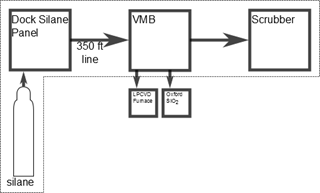
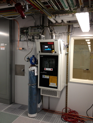
Silane Delivery System
The silane gas distribution system is responsible for safely routing and controlling the flow of silane gas from the source outside of the building to tools in the BMF. The system comprises of a silane source on the Building 2 Dock (Dock Silane), a ~350 ft long ¼’’ diameter stainless steel tubing running from the dock to a valve manifold box (VMB) inside the cleanroom. The Dock Silane panel is responsible for controlling the flow of silane to the VMB and to shut down the supply when any abnormal condition happens such as a rupture of the 350 ft long supply line. The VMB then supplies gas to the tools in the cleanroom. Finally, a Scrubber burns off the combustible gases and cracks and oxidizes reactive residual gas. During this process the silane is converted in to inert solids that are washed out in a liquid stream leaving the gas stream clean of toxic, corrosive, or combustible residue.
Toxic Gas Monitoring System (TGMS)
The cleanroom has a robust toxic gas monitoring system where gases are monitored in the exhaust of the gas cabinet where they are stored, in the exhaust of the tool, and the ambient air above the tool. Preprogrammed responses, which are tested annually, evacuate the building, notify users, and turn off gases as required if toxic gases are detected.
Silane and Ammonia Scrubber
This scrubber uses a furnace tube flooded with compressed air to decompose silane and ammonia bearing exhaust gases followed by a water rinse tower to rinse any chemical or particulate residues from the exhaust stream. The scrubbed and cooled exhaust gases are then delivered to the building acid exhaust system.
Chlorine Scrubber
The chlorine scrubber is used to treat process gasses such as Cl2, SiCl4, BCl3, and HBr. The system neutralized the toxic gasses with a chemical resin before they enter the BMF’s chemical exhaust.
Nitrogen Tank
The nitrogen tank is used to supply high purity nitrogen gas to the cleanroom and liquid nitrogen to users of the BMF and MBE labs among others.
Nitrogen Generator
The nitrogen generator is able to supply the BMF with 150,000 liters/hour of 99.5 % pure nitrogen that is used for processing.
Fire Suppression
The cleanroom is protected by a variety of systems to both detect and extinguish a fire. Detection includes the use of IR detectors in critical areas such as pyrophoric gas storage and usage as well as VESDA aspirating smoke detectors throughout all wetbenches, subfloor, and air handlers. Fire suppression includes full sprinkler coverage throughout the cleanroom, and CO2 fire suppression in all wetbenches.
Tooling and Capabilities
Lithography
ASML PAS 5500/100D Wafer Stepper: The ASML wafer stepper is a production quality lithography tool that is the main work horse for the BMF’s lithography needs. It has a Hg i-line light source and the tool has a 0.4 µm resolution with 50 nm overlay. This tool is especially useful for patterning many die on a wafer.
Heidelberg DWL2000 Pattern Generator: The DWL is an optical pattern generator designed to direct write CAD patterns on 4”, 5”, 6”, and 7” photomasks and reticles. The tool includes a robot arm that allows users to load up to 10 plates at a time. This allows the tool to write an entire set of photomasks or reticles overnight.
Heidelberg MLA 150 Maskless Aligner: The Heidelberg MLA-150 is a versatile optical lithography tool. The MLA is used to directly write a pattern onto a wafer using either a 375 nm or 405 nm laser. The tool can accommodate substrate sizes from 1 cm x 1 cm chips to 150 mm wafers, write with a resolution of 0.9 µm with an overlay of 1 µm, and has backside alignment capabilities to 0.5 µm. The MLA has decreased cycle time for rapid prototyping of designs by eliminating the need for separately manufacturing optical reticles or masks.
JEOL Electron Beam Writer: The JEOL e-beam writer is used to pattern the smallest features in the BMF. The e-beam writer has an accelerator voltage of 100,000 kV, which allows it to write feature sizes of 8 nm with a field-to-field stitching accuracy of 10 nm and a layer-to-layer overlay of 10 nm. The beam current ranges from 100 pA to 50 nA to allow writing small features accurately while being able to quickly write larger features.
Karl Suss MABA6 Mask Aligner: The MABA6 is a contact printer that can be used to transfer an image from a plate to the wafer at a 1-to-1 size with a Hg i-line light source. This tool is used for making wafer scale patterning. The MABA6 also has cameras that can be used for backside wafer alignment.
Karl Suss MJB3 Mask Aligner: The MJB3 is an additional contact printer that use a Hg i-line light source. This tool is able to accommodate thicker substrates than the MABA6.
Deposition
Lesker Lab 18: The Lab 18 is a load-locked electron beam evaporator that is the general-purpose evaporator for the BMF. The tool is able to deposit Ti, Cu, Al, Au, PdAu, Pt, Pd, Ag, and V on substrates from chip size to 150 mm wafers. Additionally, the tool is able to perform an argon RF clean on the substrate before it is loaded in the main chamber.
HTS-1: The HTS-1 system is a home built electron beam evaporator that is used for the deposition of Ti, Cu, Al, Au and PdAu. The tool can accommodate substrates from chip size up to 100 mm wafers and has the ability to preform an argon RF clean before deposition to clean substrates. This tool is used for angled evaporations and has one of the most accurate deposition rate monitors in the BMF, allowing for the deposition of very accurate film thicknesses.
PVD e-beam evaporator: The PVD evaporator is a load-locked electron beam evaporator that has been optimized to deposit uniform films over large substrates. The tool is able to deposit Ti, Cu, Al, Au, PdAu, Pt, and Ag on substrates from chip size to 150 mm wafers. Additionally, the tool is able to perform an argon RF clean on the substrate while it is loaded in the main chamber.
JoeTek: The JoeTek evaporator is a semi-automated home built 6 pocket e-beam evaporator that is specifically for high- quality evaporated aluminum Josephson and single electron transistor (SET) junctions.
CVC Evaporator: The CVC evaporator is an e-beam evaporator that is used to deposit seed layers for MBE and the deposition of magnetic materials. The CVC is able to deposit many materials including Ti, Al, Au, Ni, AuGe, Pt, Pd, SiO2, Al2O3, In, Ag, and NiCr on substrates from chip size to 3” wafers. The tool also has the ability to perform an Ar RF clean in the main chamber.
BiCu Thermal Evaporator: The BiCu system is a home built thermal evaporator that is used to deposit thick Bi layers. The BiCu system is able to deposit Bi, Cu, Al, and SiO. The tool also has the ability to perform an Ar RF clean in the main chamber.
AJA Magnetic Evaporator: The AJA Magnetic Evaporator is a dual e-beam evaporator that allows for the co-deposition of two materials. This process allows the system to deposit magnetic alloys that would not otherwise be possible to deposit. The tool can deposit Al, Cu, Ti, Ni, Fe, Au, Ag and Co on substrates from chips size to 150 mm wafers. The main chamber also has a 4 cm ion source for substrate cleaning.
Lesker SNS: The SNS system is a DC magnetron sputter tool that is dedicated to the fabrication of Josephson junctions used in the NIST 10 V standard. The system can perform an Ar RF clean on the substrate in the main chamber and can deposit Nb and Si on substrates from chip size to 150 mm wafers.
Lesker MoCu: The MoCu system is a DC magnetron sputter tool that is dedicated to the deposition of superconducting MoCu bilayers used to fabricate transition edge sensors. The system can perform an Ar RF clean on the substrate in the main chamber and can deposit Mo and Cu on substrates from chip size to 150 mm wafers.
Lesker SIS: The SIS system is a DC magnetron sputter tool that is dedicated to the deposition of superconducting / insulating / superconducting trilayers that are used to fabricate NIST SQUIDs. The system can perform an Ar RF clean on the substrate in the main chamber and can deposit Nb and Al on substrates from chip size to 150 mm wafers. To form the insulating layer, the Al is oxidized in the load lock to form aluminum oxide.
Lesker AlMn: The AlMn system is a DC magnetron sputter tool that is dedicated to the deposition of superconducting AlMn films used in the fabrication of transition edge sensors and normal metal / insulating / superconducting tunnel junctions. The system cleans the substrates with an ion mill in the main chamber and can deposit Al and AlMn on substrates from chip size to 150 mm wafers. To form the insulating layer, the Al or AlMn is oxidized in the load lock to form aluminum oxide.
AJA W: The W system is a DC and RF sputter tool that is dedicated to the deposition of W for superconducting devices. The system can perform an Ar RF clean on the substrate in the main chamber and the substrate can be heated by UV lamps during deposition. The W system can deposit W, Si, SiO2, Hf and Ti and Al on substrates from chip size to 100 mm wafers.
Lesker HiTemp: The HiTemp system is a DC magnetron sputter tool that is dedicated to the deposition of magnetic materials and other films at high temperatures. The system can perform an Ar RF clean on the substrate in the main chamber and can deposit Fe, W, Ti, Si, Nb, and AlOx on substrates from chip size to 100 mm wafers.
PVD Resistor: The PVD Resistor system is a RF sputter tool that is dedicated to the deposition of resistor material and other compatible materials. The system can perform an Ar RF clean on the substrate in the main chamber and can deposit Ti, PdAu, and MoSi on substrates from chip size to 150 mm wafers.
PVD Multi: The PVD Multi tool is a general purpose deposition system that can deposit materials through use of DC and RF sputtering and e-beam evaporation. The system has an RF sputter gun for pre-deposition cleaning of substrates and an ellipsometer to measure film thickness. The PVD Multi tool can deposit Al, Cu, Ti, Re, Au, Nb, Ni, Fe, Mo, Ge, Pt, and Pd.
PVD Big: The PVD big is a DC sputter system that is dedicated to the deposition of epitaxial Ti, TiN, Nb and Al for superconducting circuits. The system can perform an Ar RF clean on the substrate in the main chamber and has surface science characterization tools to measure characteristics of the deposited films.
Plasma Quest ECR: The ECR is a PECVD system that is used to deposit dielectric films using an electron cyclotron resonance (ECR) plasma source. The tool is dedicated to depositing insulating SiO2 films on 3” wafers. The ECR also has the ability to perform an RF clean on substrates before deposition.
Oxford ICP PECVD: The Oxford PECVD is a PECVD system that is used to deposit dielectric films using an ICP plasma source. The tool is used to deposit SiO2, SiNx, and amorphous Si films on either 3”, 100 mm or 150 mm substrates. Additionally, the tool has precision control of the substrate temperature from -150 C to 400 C by use of LN2 crossover chiller or an electric coil. Finally, the Oxford PECVD has the ability to perform an RF clean on substrates before deposition.
PVD Graphene: The Graphene system is used for PECVD of graphene, hexagonal and carbon nanotube films. The tool can heat wafers or chips to 1200 C and run CVD processes from 10 mTorr to greater than 100 Torr. The 2.45 GHz plasma, located upstream from the substrate, is designed to generate highly reactive precursor species while avoiding bombardment of the substrate.
Etch
IPE RIE: The IPE is a parallel plate RIE tool that is dedicated to etching Nb for some of the BMF’s most electrically sensitive superconducting circuits on substrates from chips to 150 mm wafers. The tool is equipped with an optical emission endpoint monitor. Approved process gasses include Ar, N2, O2, SF6, CF4, and CHF3.
Axic RIE: The Axic is a parallel plate RIE tool that is dedicated to etching SiO2 and SiNx films on substrates from chips to 150 mm wafers. The tool is equipped with a laser endpoint detector. Approved process gasses include O2, SF6, CF4, and CHF3.
STS ASE ICP DRIE: The ASE system is an ICP DRIE tool that is dedicated to deep etching Si using the Bosch process for MEMS fabrication. The tool is currently configured for 3” wafers and has a Si etch rate of about 3 µm/min.
SPTS Pegasus DRIE: The Pegasus is an ICP DRIE tool that is dedicated to deep etching Si using the Bosch process for fabrication of MEMS and micro-machined Si parts. The tool is currently configured for 150 mm wafers and has a Si etch rate of about 15 µm/min.
Trion Fl ICP: The Trion Fl system is an ICP RIE tool dedicated to etching superconducting circuits for next-generation computing. The tool is equipped with a laser endpoint detector and is configured to etch 3” wafers. Approved process gasses include SF6, CHF3, O2, and CF4.
Trion Cl ICP: The Trion Fl system is an ICP RIE tool dedicated to etching Al and TiN for superconducting devices. Since the tool is used for superconducting films, the etching of magnetic materials in not allowed. The tool is equipped with a laser endpoint detector and is configured to etch 3” wafers. Approved process gasses include Cl2, BCl3, CF4, O2, Ar, and N2.
Oxford Fl ICP: The Oxford Fl system is an ICP RIE tool dedicated to uniformly etching superconducting and dielectric films. The tool is equipped with a laser endpoint detector and is configured to etch 3” wafers. Approved process gasses include SF6, O2, and CF4.
Oxford Cl ICP: The Oxford Cl system is an ICP RIE tool dedicated to uniformly etching superconductors and III-V semiconductors such as Al, GaN, and GaAs. The tool is equipped with a laser endpoint detector and is configured to etch 3” wafers. Approved process gasses include Cl2, BCl3, HBr, O2, SiCl4, and SF6.
Plasmtaherm Fl ICP: The Plasmatherm is an ICP RIE tool dedicated to uniformly etching superconducting and dielectric films. The tool is equipped with a laser endpoint detector and is configured to etch 150 mm wafers. Approved process gasses include SF6, O2, CF4, and CHF3.
XeF2 system: The XeF2 system is a NIST constructed xenon difluoride etch system used for dry, isotropic silicon etching. The system has an internal vessel containing solid source XeF2 crystals and a video microscope for viewing etch endpoint.
Technics PE-II Asher: The PE-II is a parallel plate RIE system that is dedicated to oxygen ashing of substrates. The system can accommodate substrates from chip size to 150 mm wafers.
Intelvac Ion Mill: The Intelvac is an ion mill system that is used to remove hard to etch material from substrates. The tool is currently configured for 3” wafers and is used to remove magnetic material.
Idonus HF Vapor Phase Etcher: The Idonus Vapor Phase Etcher provides a means for users to expose substrates to an HF acid etch in a safe and simple manner. The chuck is able to accommodate substrates from chip size to 150 mm wafers. The substrate rests above a chamber containing HF and the substrate is etched by HF vapor. The substrate chuck is heated to ensure that there is no condensation of the acid on the substrate. The user does not ever handle or even see any HF acid. The system is far safer than immersion methods of HF acid etching which require handling and pouring large source bottles of acid.
Ontos Atmospheric Plasma Etcher: The Ontos system is a tool that is used for substrate surface treatment. It can remove oxygen bonds from the surface of materials and replace it with hydrogen or nitrogen bonds. This change is surface chemistry is important for further processing steps. Approved process gasses include, He, H2 in He, N2 and O2.
Thermal
Tystar Furnaces: The TYSTAR MiniTytan furnace is a bank of 4 high temperature furnace tubes used to anneal, oxidize, and perform LPCVD on either 3” of 150 mm wafers. Tube 1 is dedicated to DI steam oxidation of wafers to produce thick thermal SiO2 films. Tube 2 is dedicated to wet/dry oxidation of wafers to produce high quality thermal SiO2 films. Tube 3 is dedicated to the LPCVD of SiNx on wafers. Tube 4 is dedicated to the LPCVD of poly- crystalline Si and annealing processes.
Rapid Thermal Annealer: The Rapid Thermal Annealer is used to perform short-duration anneals on substrates from chip scale to 3” wafers. The Rapid Thermal Annealer is capable of rapid temperature increases (50 oC/s) with small overshoot and fast settling time. Its maximum operating temperature is 1200 oC. The Rapid Thermal Annealer is primarily used to anneal electrical contacts.
Despatch Polyimide Curing Oven: The Polyimide oven allows the curing of engineering polymers in an oxygen free environment. The oven includes HEPA filters to maximize cleanliness. It has a maximum temperature of 350 C and allows for slow controlled ramps of better than 1 C accuracy.
Metrology
FEI Sirion SEM: The FEI scanning electron microscope (SEM) is used for surface imaging of samples from the nm scale with a scanning electron beam of up to 30 kV. The system operates under high vacuum and can accommodate substrates from chips to 3” wafers. The SEM is a critical component in verifying features in e-beam lithography.
Nikon Microscopes: The BMF currently has 3 compound microscopes for inspection. The microscopes provide front and backside illumination, have the ability for dark-field microscopy, have built in filters and polarizers, and provide magnification from 10X – 1000X. The microscopes are computer controlled and have cameras that can take pictures that are stored on the local computer.
Leica Stereoscope: The stereoscope is useful for looking at larger objects and provides magnification from 1.6x – 12x.
Gaertner Ellipsometer: The Gaertner L116C Ellipsometer is an instrument that measures the polarization of reflected light from the surface of a wafer to determine optical and physical properties of coatings on the wafer. The system uses up to three wavelengths of laser light to determine film parameter.
Signatone Four Point Resistance Probe: The four point resistance probe is used to measure the resistance of test structures and films. It is equipped with 4 magnetic manipulators and can accommodate substrate sizes from chips to 150 mm wafers.
KLA-Tencor Alpha Step IQ Profilometer: The Alpha Step is used to measure substrate roughness to 1 Å resolution and feature heights from 10 nm to 400 µm. The tool is currently configured to measure 3”wafers.
KLA-Tencor P7 Profilometer: The P7 is a programmable profilometer used to measure feature heights from up to 357 µm with a reproducibility of 15 Å for films of 1 µm thick or less. The tool is currently configured to measure substrates from chip size to 150 mm wafers.
k-Space MOS Stress Measurement System: The k-space is a laser based Multi-beam Optical Sensor (MOS) tool used to measure thin-film stress and wafer curvature. The system is able to detect a maximum radius of curvature of 5 km. The gauges are able to measure compressive and tensile film stress from 1 MPa to 1 TPa.
Ionic Stress Gauge: The BMF currently has 2 optical stress gauges, one configured for 3” wafers, one configured for 150 mm wafers, that are used to measure stress in thin films. The gauges are able to measure compressive and tensile film stress from 1 MPa to 1 TPa.
Filmetrics F40 UV White Light Spectrophotometer: The Filmetrics is a broadband, 200 nm - 1200 nm, reflectance spectrophotometer. It can be used to measure the thickness of transparent and semi- transparent films on substrates from chip size to 150 mm wafers.
Metricon Model 2010/M Prism Coupler: The Metricon utilizes advanced optical waveguiding techniques to rapidly and accurately measure both the thickness and the refractive index/birefringence of dielectric and polymer films as well as refractive index of bulk materials. The system can accommodate substrates from chip size to 150 mm wafers. The Metricon is equipped with fixed 1064 nm, 1550 nm, and 636 nm lasers and a universal laser port for user-supplied lasers with wavelength in the 400-1600 nm range.
Process Support
Disco Dicing Saw 1: The Disco 1 is a semi-automatic dicing saw that is dedicated to dicing Si wafers. It uses diamond blades and can accommodate substrates from chip size to 150 mm wafers. It can be reconfigured as a backup to Disco 2.
Disco Dicing Saw 2: The Disco 2 is a semi-automatic dicing saw that is dedicated to dicing hard to cut substrates such as sapphire wafers. It uses resinoid blades and can accommodate substrates from chip size to 150 mm wafers. It can be reconfigured as a backup to Disco 1.
Microautomation Dicing Saw: The Microautomation is a semi-automatic dicing saw that is dedicated to dicing thick and hard to cut substrates such as sapphire wafers. It uses a variety of blades and can accommodate substrates from chip size to 150 mm wafers.
Ultron Wafer Taping System: The BMF has an Ultron wafer taping system used for dicing wafers. This system is made up of three tools. The UH114 Wafer/Frame Film Applicator mounts substrates on a dicing frame using various types of tape to prepare the substrate for dicing. After dicing, the UH104/8 UV Curing System exposes the wafer frame to UV light to reduce the adhesiveness of the UV tape. Finally, the UH130 Die Matrix Expander stretches the tape to separate the die for easy unmounting. This system can accommodate substrates from chip size to 150 mm Wafers.
Axus CMP Tool: The Axus CMP tool is dedicated to polish wafers using chemical mechanical polishing (CMP) to obtain flat surfaces across a wafer to planarize the substrate between fabrication steps. The tool is currently configured to polish SiO2 on 3” substrates.
Semiprobe Automated Wafer Probe Station: The Semiprobe is a programmable, automated wafer probe station that is used to test the electrical properties of completed devices. The system is able to measure substrates from chip size to 150 mm wafers.
Wet Benches
Wetbench 2A – EKC: The ECK bench use is dedicated to chemicals used to remove solvent resistant polymers. Approved chemicals include acetone, IPA, Novec 7200 and EKC 265.
Wetbench 2B – HF: The HF bench is an acid bench that is dedicated to HF use to etch of SiO2. Due to the dangerous nature of HF, strict safety protocols are required and a limited user base is allowed at this bench. Approved chemicals include HF 48%, BOE 6:1, and titanium etch 8-15%.
Wetbench 2C – KOH: The KOH bench is dedicated to heated KOH processing used to etch Si. Approved chemicals include KOH, NaOH, tungsten etch TFW, ammonium sulfide, and PSE-200.
Wetbench 3 – Etch: Wetbench 3 is a general purpose acid bench used to etch materials including substrate prep for GaN nanowires. Approved chemicals include HCL, phosphoric acid and IPA. The bench also has a UV ozone cleaner that is used to clean substrates.
Wetbench 4A – Etch: Wetbench 3 is a general purpose acid bench used for room temperature acid processing. Approved chemicals include Transene type A Al etch, APS0199 Cu etch, BTAH, BPS-172, nickel etchant TFB, acetic acid, and nitric acid.
Wetbench 4B – Etch: Wetbench 3 is a general purpose acid bench used for heated acid processing. Approved chemicals include Transene type A Al etch.
Wetbench 4C – Liftoff: The liftoff bench is a solvent bench that is dedicated to the removal of resists that are used for lift-off processing. Approved chemicals include NMP, acetone, IPA, methanol, and SVC 150.
Wetbench 5A – Wax: The wax bench is a solvent bench that is dedicated to waxing device wafers to carrier wafers. Approved chemicals include Crystalbond 509, acetone, IPA and Nano EBR.
Wetbench 5B – Etch: Wetbench 5B is a general purpose caustic bench used to etch materials including TiN. Approved chemicals include NH4OH and H2O2.
Wetbench 6 – 150 mm Processing: Wetbench 6 is a solvent bench that is dedicated to processing 150 mm wafers. Approved chemicals include NMP, acetone, IPA, methanol, and SVC 150.
Wetbench 7A – Strip: The strip bench is a solvent bench that is dedicated to removing photoresist from substrates. Approved chemicals include NMP, acetone, IPA, methanol, and SVC 150.
Wetbench 7B – Etch: Wetbench 7B is a general purpose acid bench used for acid processing. Approved chemicals include NanoStrip, sulfuric acid, H2O2, and gold etch TFA.
Wafer Coat 1: Wafer Coat 1 is a solvent bench that is dedicated to coating wafers with positive and negative 1 µm Hg i-line resist. This bench is equipped with an automatic spinner and an automatic hot-plate for pre-exposure bakes. Approved chemicals include SPR 660-1, AZnLOF and P20.
Wafer Coat 2: Wafer Coat 2 is a solvent bench that is dedicated to coating chips and wafers with positive 3 µm and 7 µm Hg i-line resist. This bench is equipped with an automatic spinner and an automatic hot-plate for pre-exposure bakes. Approved chemicals include SPR 660-1, SPR 220-3, SPR 220-7 AZnLOF and P20.
Wafer Coat 3: Wafer Coat 3 is a solvent bench that is dedicated to coating chips and wafers with resists that are not as clean as other resists. This bench is equipped with two programmable spinners, one for LOR resists, SU8, and PMGI, while the second is dedicated the e-beam resist HSQ. Other approved chemicals include Remover PG and P20.
Wafer Coat 4: Wafer Coat 4 is a solvent bench that is dedicated to coating chips and wafers with e-beam resists. This bench is equipped with one programmable spinner. Approved chemicals include ZEP 520A, PMMA, MMA-MAA, Espacer and Electra 92.
Wafer Develop 1: Wafer Develop 1 is a caustic bench that is dedicated to automatically developing exposed resists. This bench is equipped with an automatic spinner and an automatic hot-plate for post-exposure bakes. Approved chemicals include MF26A and DX-40.
Wafer Develop 2: Wafer Develop 2 is a caustic bench that is dedicated to hand developing exposed resists. This bench is equipped with a cold plate to allow for below room temperature developing of resists. Approved chemicals include MF26A, AZ developer, AZ 400k, DX-40, ZED, MIBK, IPA, and O-xylene.
Reticle Develop: Reticle Develop is an acid and caustic bench that is dedicated to developing and etching photomasks and reticles. Approved chemicals include Microposit Developer and CR7-S chrome etch.
Reticle Strip: Reticle Strip is a solvent bench that is dedicated to removing photoresist from photomasks and reticles. The bench is equipped with two heated ultrasonic baths filled with Remover 1112A. Other approved chemicals include acetone, IPA and CD40 mask cleaner.
Fume Hood: The fume hood is located in a service chase and is used to clean parts and other objects from the main cleanroom. Approved chemicals include acetone, IPA, NMP and other commercial cleaners.
Plating Bench: The plating bench is an acid bench that is located in process support outside of the main cleanroom that is dedicated to plating metals onto substrates. Currently, the bench has chemicals that are capable of plating Au, Cu, and Bi.
Process Support Acid Bench: The process support acid bench is a general purpose acid bench located in process support. It is used to etch circuit boards and clean post-process wafers. Approved chemicals include ferric chloride, acetone, IPA, hydrochloric acid, nitric acid, phosphoric acid, and acetic acid.
Process Support Solvent Bench: The process support solvent bench is a solvent bench located in process support. It is used to make PDMS structures and to clean post-process wafers. Approved chemicals include NMP, acetone, IPA, methanol and PDMS.
Other
Spin Rinser Dryers: The BMF has several spin rinser dryers that can be used to clean wafers, photomasks, and reticle plates. The spin rinser dryers can accommodate 3” and 150 mm wafers and 4”, 5”, 6” and 7” photomasks and reticle plates.
Western Magnum XRL-120 Laminator: The laminator is a tool that is used to coat substrates with roll- on photoresist. The tool is currently configured with MX5020 and can accommodate other resists.