
Official websites use .gov
A .gov website belongs to an official government organization in the United States.
Secure .gov websites use HTTPS
A lock (
) or https:// means you’ve safely connected to the .gov website. Share sensitive information only on official, secure websites.
Summary
Many, if not all, of the performance and reliability metrics of semiconductor devices (power electronics through advanced electronics) have macroscale characteristics (currents, voltages, capacitances) which are limited by nano-scale imperfections (defects). These nano-scale and in many cases atomic-scale defects can be interrogated using magnetic resonance spectroscopy.
Our magnetic resonance spectroscopy effort strives to be at the forefront of understanding the roles that critical atomic-scale defects play in determining device performance and resiliency. The combination of our electron spin based magnetic resonance and solid-state device electrical characterization skill sets are highly unique and place us in an exceptional position to deliver truly fundamental physical understandings. It’s this kind of knowledge that is required to advance immature technologies and associated metrology into practical reality.
Description
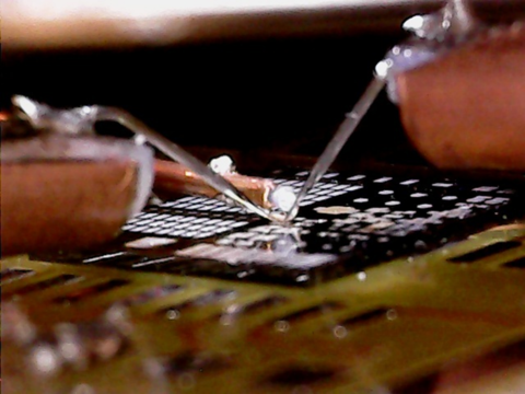
Custom-built wafer level probes in position to perform EDMR measurements on fully processed transistors.
Custom-built wafer level probes in position to perform EDMR measurements on fully processed transistors.
Electronics are all around us and have completely reinvented nearly every aspect of our society. Virtually any system, large or small, contains some type of electronics that may or may not be directly visible to the user. Our insatiable appetite for faster and better technology has been fueled by the tremendous progress and innovation made in advancing the fundamental building blocks of electronic circuity.
These electronic devices advance extremely quickly with new technologies, materials, and architectures always on the horizon, each with their own unique challenges. Thus, there is an ever present need to understand new physical phenomena and their underlying atomic-scale origins. Accomplishing this task requires a strong and fundamental understanding of: (1) the underlying physics of device operation, (2) the chemical and physical nature of atomic-scale defects and imperfections, and (3) the metrology tools and their associated phenomena that are used to interrogate the problems.
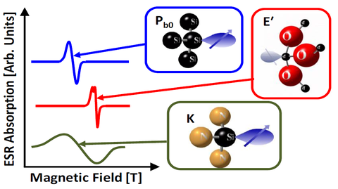
Our magnetic resonance spectroscopy effort leverages the most powerful analytical tool available to accomplish this goal; electron spin/paramagnetic resonance spectroscopy (ESR/EPR). In addition to conventionally detected ESR/EPR suitable for larger area “bulk” samples, we employ several highly specialized electrically detected magnetic resonance (EDMR) schemes that allows detailed spectroscopic information to be obtained in fully-processed individual device structures. Finally, we also link the atomic-scale defect information obtained via ESR/EPR/EDMR to actual device performance and operation via a multitude of conventional device-level electrical measurements (current versus voltage, capacitance versus voltage, charge pumping, etc.).
RESEARCH OPPORTUNITIES
Please contact jason.ryan [at] nist.gov (Dr. Jason Ryan) directly to discuss collaborations or research positions related to magnetic resonance spectroscopy and/or advanced electrical characterization of various electronic materials and devices. Additionally, qualified U.S. Citizen candidates are encouraged to contact jason.ryan [at] nist.gov (Dr. Ryan) regarding NRC research and fellowship programs at NIST (https://ra.nas.edu/RAPLab10/Opportunity/Program.aspx?LabCode=50)