

Official websites use .gov
A .gov website belongs to an official government organization in the United States.

Secure .gov websites use HTTPS
A lock (
) or https:// means you’ve safely connected to the .gov website. Share sensitive information only on official, secure websites.


Electronics for Cryogenic Environments
Summary
There is a continued motivation to scale towards meaningful quantum computation—on the order of one million qubits. The cryogenic electronics program designs and develops the as-yet unrealized metrology needed to develop a class of custom cryogenic integrated circuits needed to support the quantum computation scale-up. These custom circuits must be specially engineered to operate efficiently at cryogenic temperatures, consume exceptionally low power, deliver exquisitely timed (multiplexed) input/output excitation signals, and reliably amplify the miniscule quantum readout signals. While this circuit functionality is commonly realized at room temperatures, translating these circuit architectures to the cryogenic environment presents severe engineering challenges. While the research is largely driven by quantum applications, the cryogenic device and circuit infrastructure also supports the aerospace Industry, high-performance computing, and nearly all base standards and applied precision measurements (quantum current standards, quantum hall resistance standards, single and few photon counting, etc.)
Description
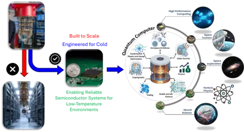
The metrology developed in this program enables the crucial inclusion of circuit functionality at cryogenic temperatures to enable scaling of quantum computation to meaningful levels.
The operation of electronics optimized for room temperature applications in cryogenic environments introduces a remarkable number of physical and engineering hurdles. It is unsurprising that devices and circuits designed for room temperature encounter shifts in their operation parameters in cryogenic environments.
Compensation of these temperature-induced parametric shifts are relatively well understood and may be remedied with engineered workaround solutions. However, large thermal excursions also introduce a variety of new physical phenomena which impact overall performance, reliability, and design-dependent thermal gradients.
The Electronics for Cryogenic Environments (ECE) program develops electrical methods to quantify these new cryogenic peculiarities and imbue this understanding into application-specific circuits specifically designed to reliably handle cryogenic operation. The depth of characterization detail will far exceed the norm and will rely on exhaustive temperature-dependent device and circuit electrical characterizations of everything from commercial off the shelf components to custom designs in the most advanced technology nodes.
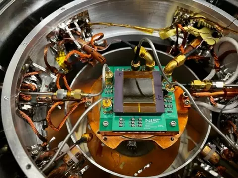
These unique circuit requirements are motivated largely by the maturation of the quantum information science landscape.
Initialization, manipulation, and readout of large arrays of fragile quantum states requires the help of complex cryogenic analog and digital control and sensing electronics to eliminate input/output thermal constraints and noise decoupling.
Unfortunately, these cryogenic electronics are strongly design/materials/processing-dependent and relegated to proprietary industrial efforts. The ECE efforts will instead be disseminated both internally and externally whenever possible. Though quantum concerns are the primary motivation, there are also clear links to the aerospace and high-performance computing spaces.