Summary
Since its discovery, graphene, a single atomic sheet of carbon atoms, has become a leading contender to be a key building-block material for future generations of extraordinarily fast electronic devices. Electrons travel through this novel material like light waves, with less disturbance at room temperature than any other known substance. This high carrier mobility results from the fundamental symmetry of the graphene honeycomb lattice. Defects in the graphene lattice can affect the physical properties of graphene in unexpected ways, and harnessing the influence of these defects may be one method to control both the material's strength and electrical properties. The goals of this project are to characterize the defects found in the production of graphene on the atomic scale with scanning tunneling microscopy and spectroscopy measurements (STM/S) in order to gain insight into the electronic properties of graphene.
Description

The graphene honeycomb lattice is a key element in determining many of graphene's spectacular properties, which are desirable for a host of electronic applications. The graphene 6-fold symmetric lattice gives rise to charge carriers behaving like light-waves having zero mass. The charge carriers in graphene have new additional quantum mechanical properties, which allow the carriers to zip through potential disturbances without scattering and result in enhanced electrical carrier mobility. Certain defects can affect the graphene carriers more than others. In particular, atomic-scale defects in the graphene lattice can cause significant scattering of the graphene charge carriers, and lead to a loss of carrier mobility in electronic applications.
This project applies NIST's unique nanoscale measurement instrumentation and expertise to support the development of graphene-based future electronics. One aim is to determine the properties that underlie the high-speed movement of electrons in graphene and how that movement might be affected by structural defects that arise both within single graphene sheets and at boundaries with other materials. The project also aims to evaluate a promising "wafer scale" method for making high-quality graphene, an achievement that could greatly accelerate the commercialization of graphene-based devices.
The research effort includes work on refining promising methods for manufacturing graphene on a commercial scale. These methods in epitaxial growth of graphene on silicon carbide (SiC) substrates, and chemical vapor deposition of graphene on metal foils. In epitaxial growth of graphene on SiC, large sheets of graphene are prepared by evaporating silicon from wafers of SiC. As the silicon evaporates, it leaves behind atom-thick layers of carbon in the graphene structure that are stacked atop the SiC that remains. Project scientists use custom-built scanning tunneling microscopes in the NIST Center for Nanoscale Science and Technology to measure both physical surface features and the behavior of electrons scattering from atoms and defects in the crystal. These unique, custom-built instruments make it possible to image the atomic structure of the graphene lattice, the structure of defects, and how the charge carriers scatter from the defects.
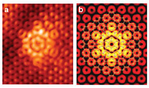
The team discovered that a new class of topological defects forms in the graphene hexagonal lattice from the decomposition of SiC in ultra-high vacuum. These defects form closed circular loops with flower-like patterns (Fig. 1). The threefold carbon bonding in graphene permits defective rings to form, comprising either 5 or 7 atoms instead of 6, that can be strung together in extended structures to form linear grain boundaries. The NIST researchers have shown that the same 5 and 7 atom rings can be linked together to form closed loops defining an unusual type of rotational grain boundaries. The smallest member of this flower family has been observed in STM images of graphene grown on SiC [Fig. 1(a)], and theoretical calculations [Fig. 1(b)] indicate it is one of the lowest energy defects in the graphene lattice, explaining its tendency to form during the high temperature processing used to make graphene from SiC.

Defects in the graphene lattice scatter electron waves and create ripple-like patterns, much like posts in water scatter a wave. Project scientists have used scanning tunneling spectroscopy to measure these interference patterns originating from lattice defects in the graphene electron system. By measuring the distance between the ripples, the NIST researchers confirmed the predicted light-like dispersion of graphene's charge carriers.
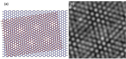
A different type of interference pattern can occur when two layers of graphene are stacked on top of each other. A moiré pattern appears in the stacked layers when there is a rotation of one lattice relative to the other [Fig. 2(a)]. NIST researchers measured the moiré patterns in stacked graphene layers [Fig. 2(b)], demonstrating that these patterns can be used to determine degree of strain in the graphene lattice. The different ways to stack graphene layers can lead to profound effects in the electronic properties of the individual layers, which NIST researchers are ming with magneto-electronic measurements.

Selected Publications
- Grain boundary loops in graphene, E. Cockayne, G. M. Rutter, N. P. Guisinger, J. N. Crain, P. N. First, and J. A. Stroscio, Physical Review B 83, 195425 (2011).
NIST Publication Database Journal Web Site - Imaging the interface of epitaxial graphene with silicon carbide via scanning tunneling microscopy, G. M. Rutter, N. P. Guisinger, J. N. Crain, E. A. A. Jarvis, M. D. Stiles, T. Li, P. N. First, and J. A. Stroscio, Physical Review B 76, (2007).
NIST Publication Database Journal Web Site - Scattering and interference in epitaxial graphene, G. M. Rutter, J. N. Crain, N. P. Guisinger, T. Li, P. N. First, and J. A. Stroscio, Science 317, 219-222 (2007).
NIST Publication Database Journal Web Site - Structural analysis of multilayer graphene via atomic moiré interferometry, D. L. Miller, K. D. Kubista, G. M. Rutter, M. Ruan, W. A. deHeer, P. N. First, and J. A. Stroscio, Physical Review B 81, 125427 (2010).
NIST Publication Database Journal Web Site Edge structure of epitaxial graphene islands, G. M. Rutter, N. P. Guisinger, J. N. Crain, P. N. First, and J. A. Stroscio, Physical Review B 81, 245408 (2010).
NIST Publication Database Journal Web SiteMore

