For electrical charges racing through an atom-thick sheet of graphene, occasional hills and valleys are no big deal, but the potholes—single-atom defects in the crystal—they're killers. That's one of the conclusions reached by researchers from the National Institute of Standards and Technology (NIST) and the Georgia Institute of Technology who created detailed maps of electron interference patterns in graphene to understand how defects in the two-dimensional carbon crystal affect charge flow through the material. The results, appearing in the July 13 issue of Science, have implications for the design of graphene-based nanoelectronics.
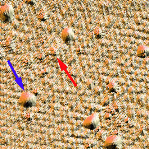
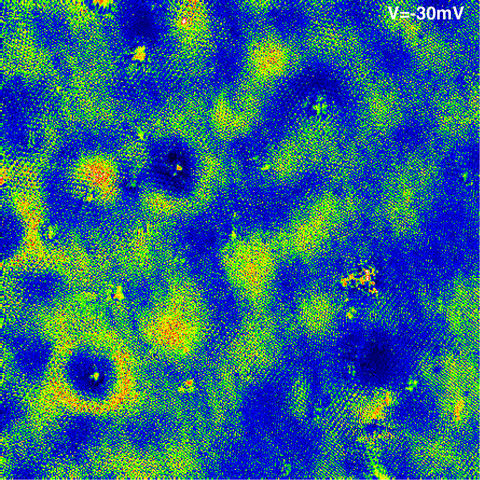
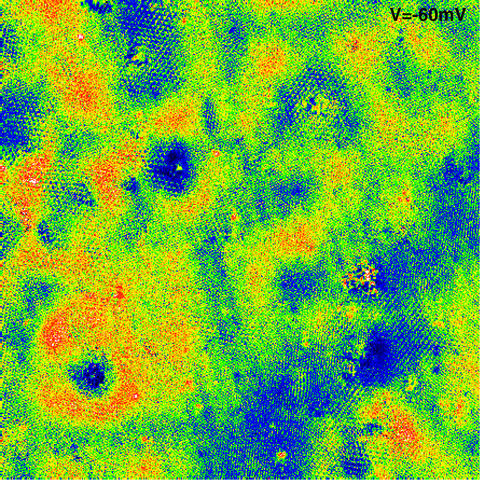
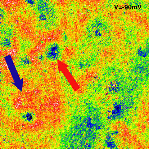
BELOW: A comparison of an STM topographic image of a section of graphene sheet (top left) with spectroscopy images of electron interference at three different energies shows strong interference patterns generated by atomic scale defects in the graphene crystal (red arrows) but only modest disturbances caused by larger scale bumps in the sheet (blue arrows.) Analysis of the ripples shows that the electron energy in graphene is inversely proportional to its wavelength, just like light waves. The area imaged is approximately 40 nanometers square.


A single layer of carbon atoms tightly arranged in a honeycomb pattern, graphene was long thought to be an interesting theoretical concept that was impossible in practice—it would be too unstable, and crumple into some other configuration. The discovery, in 2004, that graphene actually could exist touched off a rush of experimentation to explore its properties. Graphene has been described as a carbon nanotube unrolled, and shares some of the unique properties of nanotubes. In particular, it's a so-called ballistic conductor, meaning that electrons flow through it at high speed, like photons through a vacuum, with virtually no collisions with the atoms in the crystal. This makes it a potentially outstanding conductor for wires and other elements in nanoscale electronics.
Defects or irregularities in the graphene crystal, however, can cause the electrons to bounce back or scatter, the equivalent of electrical resistance, so one key issue is just what sort of defects cause scattering, and how much? To answer this, the NIST-Georgia Tech team grew layers of graphene on wafers of silicon carbide crystals and mapped the sheets with a custom-built scanning tunneling microscope (STM) in the NIST Center for Nanoscale Science and Technology that can measure both physical surface features and the interference patterns caused by electrons scattering in the crystal. (Graphene on silicon carbide is a leading candidate for graphene-based nanoelectronics.)
The results are counter-intuitive. Irregularities in the underlying silicon carbide cause bumps and dips in the graphene sheet that lies over it rather like a blanket on a lumpy bed, but these relatively large bumps have only a minor effect on the electron's passage. In contrast, missing carbon atoms in the crystal lattice cause strong scattering, the interference patterns rippling around them like waves hitting the piles of a pier. From a detailed analysis of these interference patterns, the team verified that electrons in the graphene sheet behave like photons, even at the nanometer scale.
This work is supported in part by the Office of Naval Research, National Science Foundation and Intel Research.
G.M. Rutter, J.N. Crain, N.P. Guisinger, T. Li, P.N. First and J.A. Stroscio. Scattering and interference in epitaxial graphene. Science 13 July 2007.

