Official websites use .gov
A .gov website belongs to an official government organization in the United States.
Secure .gov websites use HTTPS
A lock (
) or https:// means you’ve safely connected to the .gov website. Share sensitive information only on official, secure websites.
Summary
Crystalline silicon is a desirable host material for solid state qubits due to potential for electrically controlled interactions between exquisitely isolated qubits and the possibility of leveraging the massive silicon microelectronics industry. Silicon can be made better for hosting qubits by enriching the dominant 28Si isotope (nuclear spin I = 0) and depleting 29Si with I = ½ that can cause decoherence. As highlighted below, we have developed novel methods for growing 28Si epilayers on top of a natural abundance silicon substrates to explore these benefits. Our 28Si epilayers can be enriched to any arbitrary, preselected level of 28Si from natural abundance to above 99.9999%, making it the most highly enriched silicon in the world. To investigate whether increasing enrichment continues to increase quantum benefit throughout this entire range, we are making MOS Hall bars and quantum dot devices that can be used as diagnostic qubits for benchmarking enrichment level or other process variations. Finally, we are exploring hybrid silicon materials using super-saturated doping in hopes of creating regions of superconductivity within crystalline silicon, thereby merging super- and semiconducting devices in a monocrystalline system. Links to related publications can be found on the right sidebar.
Description
Enriching silicon from 5% to <1 ppm 29Si
Groundbreaking work around the world has realized qubits in silicon using metal-oxide-semiconductor (MOS) devices, single atomic dopants/defects and SiGe heterostructures, and, in all cases, the qubit coherence and fidelity properties are improved when using enriched silicon. In these cases, the benefit seems to scale proportionally with the reduction in 29Si density, but at some point the benefit is expected to diminish as other decoherence mechanisms remain. Theoretical models have provided guiding predictions, but some recent experiments have unexpectedly shown better performance than predicted.
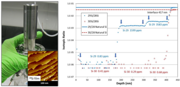
In our project, we have developed the capability to epitaxially deposit ultra-enriched 28Si (<100 ppb 29Si) by ionizing commercial silane gas and using a magnetic sector analyzer to separate the isotopes before deposition. Shown in Figure 1 is a ultra-high vacuum (UHV) ionization source we developed to accomplish the ionization, while maintaining extremely clean growth conditions. An example of a scanning tunneling microscope (STM) image of a single-crystal 28Si epitixial film is shown as well, demonstrating the material readiness for device fabrication. We have also shown the ability to deposit films with a pre-selected enrichment ranging from natural abundance to <1 ppm 29Si, providing a framework for evaluating the relationship between enrichment and coherence. As an example, the right side of Figure 1 shows a Secondary Ion Mass Spectroscopy (SIMS) depth profile of an enriched silicon sample with three different enrichment levels, selected by changing the process tuning in real-time. In a recent paper (right sidebar) we demonstrated the capability to deposit enriched silicon at a preselected value over many orders of magnitude in enrichment.
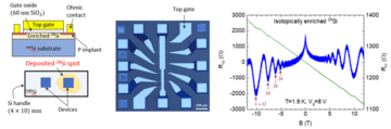
Quantum transport effects in enriched MOS Hall bars
As a means of characterizing the electrical performance of our ultra-enriched silicon, and also as a framework for seeking “simple” predictive indicators for device performance in the quantum dot regime, we fabricated MOSFET Hall bar devices for cyrogenic transport studies. Since many fabrication process factors besides the material quality can influence the ultimate device performance, we chose to fabricate devices on the same chip that were both on the enriched silicon and on the float zone handle, as shown in the lower left of Figure 2. Both devices showed very high mobilities, with the enriched silicon’s mobility about a factor of three less than the float zone device. Additionally, well developed Shubnikov-de Haas oscillations (Figure 2 right) are visible in both natural abundance and enriched silicon, enabling analysis of the underlying scattering mechanisms as discussed in the full paper (link at right).
Toward diagnostic MOS quantum dot devices
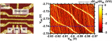
In addition to macro scale devices for material characterization, we are developing quantum dot devices intended to be diagnostic qubits. Specifically, we are developing devices capable of functioning in the single electron regime as quantum dots, putting a priority on fabrication simplicity and minimizing device failure mechanisms rather than ability function as a quantum processor. Faster turnaround devices can help optimize materials and processes for implementation in more complex, fully functional qubit devices.
An example of our first generation of these devices is shown in Figure 3, the left side is an AFM image revealing the Ti/Pd gate layer structure. The device is designed as two double quantum dots with mirror image alignment at top and bottom for charge sensing. The upper and lower horizontal wire gates are connected to Ohmics so that they can be used to invert an electron gas beneath them and carry current in the silicon beneath the gate. The single-ended gates coming in from top and bottom are used for repulsive fields that introduce tunnel barriers in the inverted regions of the adjacent channel, thereby forming one or two quantum dots in each channel. The middle horizontal gate can then be used for squeezing the dots, or other global manipulations. These devices can successfully charge sense each other, as shown in Figure 3 right, where the current in the upper quantum dot device is used to sense the charge transitions in the lower quantum dot. The bright lines indicate charge stability boundaries where one additional electron is loaded onto the lower quantum dot.
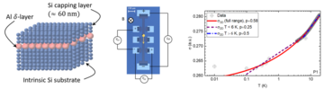
Al delta-doped silicon as a possible super-semiconductor hybrid
Another strategy for making quantum devices in silicon is to use controlled regions of doping to generate conduction rather than external fields controlled by gates. Perhaps most prominently, phosphorus doping has been used to create single atom transistors and other devices where dopants were used for all conducting elements. Also, boron and gallium have been used to generate superconductivity within silicon crystals at high doping densities, and theoretical work has predicted aluminum can also be used for synthesizing superconducting silicon at sufficiently high doping densities in silicon. Aluminum has a nuclear mass closer to silicon, which may reduce local strain, as well as a predicted higher critical temperature for superconductivity, making it desirable to explore. Additionally, using holes as charge carriers avoids the complications of the electron’s “valley” degeneracy.
Using MBE techniques within our silicon deposition system, we have synthesized Al delta layers (Figure 4 left) within crystalline silicon that remains conducting to milliKelvin temperatures. In bulk systems, Al is reported to have little or no solubility in silicon, so it was not apparent in advance achieving conduction was even possible. In order to study the nature of the conduction in these layers, we mesa etched Hall bar devices (Figure 4 center) and cooled them to cryogenic temperatures. We find carrier densities similar to the dopant density and carrier mobilities similar to other dopant-based delta layer systems. Given this success, we cooled to milliKelvin temperatures and did not see evidence of superconductivity. Using the temperature dependent weak localization (Figure 4 right), we found the conduction is not consistent with 2D conduction, suggesting dopants have spread out and have a density less than needed for superconductivity. Ongoing efforts are aimed at better confining the dopant spread. Additional information can be found in the paper linked at right.