
Official websites use .gov
A .gov website belongs to an official government organization in the United States.
Secure .gov websites use HTTPS
A lock (
) or https:// means you’ve safely connected to the .gov website. Share sensitive information only on official, secure websites.
Energy and Environment: Highlights
1970: Improving Antenna Design and Performance
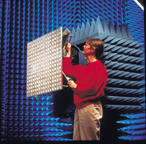
The 1,000 satellites orbiting the Earth today would be space junk without high-performance, cost-effective antennas to transmit and receive communications signals. Among NIST's pivotal contributions to antenna technology was the development of a theory that made it practical for researchers to compute an antenna's complex outdoor radiation pattern using data collected entirely indoors near a test antenna. (Photo at right shows an antenna being readied for near-field measurements.)
NIST also developed software for using the data to compute field performance; the source code remains in use today. These advances have saved millions of dollars in testing costs for the military and satellite manufacturers, among other users.
1971: A New Kind of Microscope
The scanning tunneling microscope (STM), widely used today in fields ranging from molecular biology to nanotechnology, enables scientists to see and manipulate individual atoms on surfaces and understand some of the physical, electronic, and magnetic structures of surfaces. It is such an important tool that, in 1986, two IBM Corp. scientists shared the Nobel Prize in physics for building the first STM able to glimpse the atomic surface. Today, there are about 5,000 STMs and related instruments in use throughout the world.
Some 15 years before, NIST physicist Russell Young built the Topografiner (left), a novel microscope that surveyed surfaces in great detail, nearly to the level of individual atoms. With this instrument, Institute researchers demonstrated the operating principle of the STM. The Nobel committee credited Young with being the first to demonstrate the use of a sharp-tipped stylus, held at a very small and constant distance above a sample, to scan and map surfaces. The committee also recognized Young for proposing to use "tunneling" current—a quantum mechanical phenomenon—as the means to image surfaces. Today, the Topografiner resides in the Smithsonian Institution.
Young's work is a highlight of extensive NIST research on surfaces, sometimes described as a fourth state of matter because they are so different from solids, liquids, and gases. Rapid advances in surface science at NIST and elsewhere from the 1960s through the present have contributed to the development of catalysts, semiconductor devices, chemical sensors, and computing systems. In 1985, for example, Institute researchers demonstrated magnetic imaging using scanning electron microscopy with polarization analysis (SEMPA), a new type of microscopy they developed to observe magnetic structures up to 100 times smaller than can be seen using optical techniques. Since then, SEMPA has assisted in the rapid development of high-density magnetic data-storage systems.
1971: The Origins of Closed Captioning
In an example of a research technology with significant commercial spin-offs, NIST's TvTime, a method for broadcasting time and frequency information on television, was transformed into closed captioning. Approved for wide use by the Federal Communications Commission in 1976, the technology won an Emmy Award for outstanding achievement in engineering development in 1980. It has greatly benefited the deaf and hard of hearing. Today, closed captioning is used on virtually all nationally broadcast programming, most new syndicated programming, many cable programs, and thousands of motion pictures. It also created a new industry of suppliers of closed captioning services.
1972: Making Better Measurements
Measurements have a symbiotic relationship with science and technology. They depend on each other, and if one advances, the other does too.
A case in point is the work of Ken Evenson and his team at NIST's Boulder campus, who made a world-record measurement of the frequency of laser light in 1972. That led to a much more accurate value for the speed of light, thus enabling scientists to better understand the behavior of the universe and more accurately track satellites and spaceships. The ripple effect of the advance then came back full circle to measurement science in the form of a new, more stable definition of the meter.
NIST actually achieved nine world-record measurements of laser frequency between 1969 and 1979. But the one in 1972 was special because the laser was stabilized, ensuring that any other similar laser will operate at the same frequency so that the experiment can be repeated. This design also enabled accurate independent measurements of the light's wavelength.
Wavelength multiplied by frequency equals the speed of light—which in this case was 100 times more accurate than the value accepted for the previous 15 years. The new value for the speed of light was accepted internationally in 1973 (and finalized in the 1983 redefinition of the meter).
Because frequency can be measured more accurately than wavelength (in fact, frequency is the most accurately measured value in science), scientists then wanted to improve the standard of length, which had been defined in terms of the wavelength of a certain type of light. In 1983, based largely on the achievements of Evenson and his team, the meter was formally redefined in terms of the new value for the speed of light.
1977: Safeguarding Electronic Data
About the time the personal computer was invented, NIST issued the first publicly available data encryption standard (DES)—a landmark event in an era when most cryptographic equipment was either proprietary or classified.
DES has secured much of the world's electronic data ever since. It was the first cryptographic algorithm endorsed by the federal government and was embraced by the private sector, especially banking, where it protects billions of dollars in transfers and other financial transactions daily. When a person withdraws cash from an automated teller machine, for instance, his or her personal identification number is probably encrypted using DES.
Reflecting the popularity of DES, four leading standards-setting organizations participated in the development of DES-based cryptographic standards for financial data, information processing and financial services, federal procurement, and telecommunications security.Commercial hardware and software products also rely on it. The most recent industry survey showed that, as of late 1997, almost half of U.S. cryptographic products and 43 percent of foreign products used DES.
The DES algorithm was developed by IBM Corp. However, NIST played a major role in the resulting popularity of the technology by making it a standard for federal agencies, assuring that the standard met all requirements and was acceptable to many potential users, analyzing security concerns, and evaluating the costs and benefits of modifying or replacing the standard. The thoroughness of the testing is reflected by the fact that, even 23 years after it was issued, DES is still considered unbreakable except by brute force (i.e., using computers to try every possible 56-bit key). Today, NIST is coordinating the development of a more powerful successor standard.
1979: In Semiconductors, Smaller Is Better
As integrated circuits (computer chips) shrink in size, the semiconductor industry needs increasingly tiny "rulers" for measuring the widths of circuit features. If feature size is not controlled, then the chips may fail. Who better to meet this need than NIST, which has assisted the semiconductor industry for more than 45 years?
When the feature-size issue first arose, NIST created an entirely new measurement system and, in 1979, issued its first photomask linewidth standard, which became an instant best seller. Three leading companies stopped using internal standards and adopted the one from NIST. This standard reduced measurement discrepancies among companies tenfold, stimulated the production of new commercial instruments, extended the range of use of optical microscopes, and saved the industry millions of dollars annually.
By the mid-1980s, chip features were on the order of 1 micrometer wide (75 to 100 times thinner than a human hair). Today, dimensions are about one-tenth that size. To meet today's needs, NIST has responded with photomask linewidth standards with ever smaller features, as well as several new approaches for accurately measuring circuit features as small as one-tenth of a micrometer (or less). Methods that use the spacing between crystalline silicon atoms or direct counting of the atoms as the ruler are currently being pursued. NIST researchers also are developing special microscopic techniques for use as calibration and metrology tools.
| Notice of Online Archive: This page is no longer being updated and remains online for informational and historical purposes only. The information is accurate as of 2001. For questions about page contents, please inquiries [at] nist.gov (contact us). |