
Official websites use .gov
A .gov website belongs to an official government organization in the United States.
Secure .gov websites use HTTPS
A lock (
) or https:// means you’ve safely connected to the .gov website. Share sensitive information only on official, secure websites.
Advanced Metrology to Enable Next Generation EUV Photoresists
Summary
The semiconductor industry continues to push for smaller features, more integration, and increased yield. New photoresist chemistries and advances in extreme ultraviolet lithography are enabling this trend. Focusing on new photoresist chemistries and extreme ultraviolet (EUV) lithography, the team at NIST plans to develop advanced metrology for advanced high-NA photoresist technology that will benefit future microelectronics manufacturing.
This project will offer industry a roadmap for rapid characterization of new EUV resist formulations, enhancing manufacturing yield and boosting competitiveness in the US semiconductor sector.
Grand Challenge 2. Advanced Metrology for Future Microelectronics Manufacturing
Description
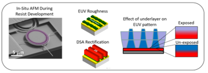
A combination of in situ developmental monitoring, and soft X-ray measurements will provide information on the EUV latent image and roughness at all stages of the development process. Latent image measurements through soft X-rays will inform the role of exposure on the photoresist and how roughness changes throughout
EUV (extreme ultraviolet) lithography, the technology that “saved Moore’s Law,” is widely regarded as the future of cutting-edge nanofabrication. It was developed in the United States and U.S. companies in many parts of the EUV ecosystem have established dominance in the field that must be defended and grown.
The advent of EUV has been accompanied by new challenges in high volume manufacturing. To increase throughput and lower cost, EUV fabs want to minimize dose, but they risk increasing photon shot noise and underexposing the resist, both of which increase line edge roughness (LER), which lowers yield. Given this, and many other technical challenges, it is evident that the semiconductor industry will greatly benefit from new, advanced capabilities in measuring lateral and vertical chemical heterogeneity across EUV processes.
EUV lithography is the foundation of all recent and foreseeable future advancements for semiconductor manufacturing and underpins progress in essentially all of the CHIPS R&D Grand Challenges.
This project will provide industry with new unique NIST measurement capabilities. This includes:
- Soft X-ray whole film spectroscopy and vertical depth profiling for photoresists and underlayers.
- EUV latent image characterization using soft X-ray scattering.
- Characterization of block copolymers for EUV pattern rectification.
- Real-time AFM probe methods for monitoring of photoresist development.
Providing industry with these new capabilities will enable technological advantages for the formulation and processing of advanced EUV and high-NA EUV photoresists, which will help industry develop pathways to meet LER targets. Reducing LER and stochastic defects in high-NA EUV resists is of paramount importance to the semiconductor industry.
Success of this project will ultimately increase semiconductor device manufacturing throughput and yield for devices of reduced feature sizes. These advantages will greatly advance the competitiveness and accelerate high-volume manufacturing in the U.S. semiconductor industry.