R Joseph Kline (Fed)
Research Interests
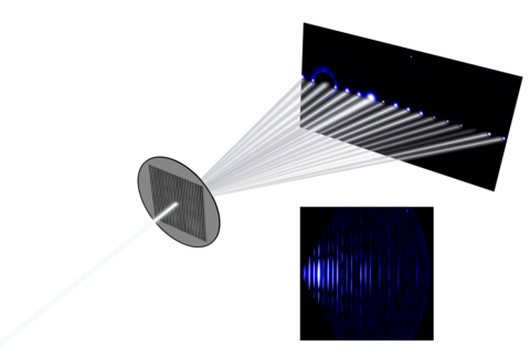
My research involves developing methods for X-ray metrology for complex 3D nanostructures for the semiconductor industry. I also develop methods for using soft and hard x-ray scattering to characterize the pattern shape and local chemistry in next generation lithographies such as directed-self assembly of block copolymers and extreme ultraviolet lithography. A method developed by our group called critical dimension small angle X-ray scattering (CDSAXS) was recently transferred to the semiconductor industry and is being used in memory fabs for characterizing high aspect ratio memory structures such as 3D-NAND. I am currently the project leader of the Metrology for Nanolithography project.

Professional Service
- Advanced Light Source (ALS) - Proposal Study Panel 2018-present
- Advanced Photon Source (APS) - User Organization Executive Committee (Chair 2018) 2016-2019
- Advanced Photon Source (APS) - Chem/Mat/Bio Proposal Review Panel
- Stanford Synchrotron Radiation Lightsource (SSRL) - User Organization Executive Committee
Research Opportunities
National Research Council Postdoctoral Fellowship – Open to U.S. citizens with an annual stipend of $72,750 per year. Applications are due on either Feb. 1 or Aug. 1. Contact me if interested in an NRC post-doc for researching dimensional metrology for nanoelectronics, directed self-assembly of block copolymers, or X-ray scattering of polymers.
Selected Publications
- “Buried Structure in Block Copolymer Films Revealed by Soft X-ray Reflectivity,” D.F. Sunday, J.L. Thelen, C. Zhou, J. Ren, P.F. Nealey, R.J. Kline, ACS Nano, 15, 6, 2021, 9577-9587 <Link>
- “Influence of Additives on the Interfacial Width and Line Edge Roughness in Block Copolymer Lithography,” D.F. Sunday, X. Chen, T.R. Albrecht, D. Nowak, P.R. Delgadillo, T. Dazai, K. Miyagi, T. Maehashi, A. Yamazaki, P.F. Nealey, R.J. Kline, Chem. Mater. 32 (8), 2020, 2399-2407 <Link>
- “X-ray characterization of contact holes for block copolymer lithography,” D.F. Sunday, F. Delachat, A. Gharbi, G. Freychet, C.D. Liman, R. Tiron, R.J. Kline, J. Appl. Cryst. 52 (1), 2019, 106-114 <Link>
- “Metrology for the next generation of semiconductor devices,” N.G. Orji, M. Badaroglu, B.M. Barnes, C. Beitia, B.D. Bunday, U. Celano, R.J. Kline, M. Neisser, Y. Obeng, A.E. Vladar, Nature Electronics, 1 (10), 2018, 532-547 <Link>
- "Determination of the Internal Morphology of Nanostructures Patterned by Directed Self Assembly," D.F. Sunday, M.R. Hammond, C. Wang, W.L. Wu, D.M. DeLongchamp, M. Tjio, J.Y. Cheng, J.W. Pitera, R.J. Kline, ACS Nano, 8 (8), 2014, 8426-8437 <Link>
- "Molecular Origin of High Field-Effect Mobility in an Indacenodithiophene-Benzothiadiazole Copolymer," X. Zhang, H. Bronstein, A.J. Kronemeijer, J. Smith, Y. Kim, R.J. Kline, L.J. Richter, T.D. Anthopoulos, H. Sirringhaus, K. Song, M. Heeney, W. Zhang, I. McCulloch, D.M. DeLongchamp, Nature Comm. 4, 2013, 2238 <Link>
- "Contact-induced crystallinity for high-performance soluble acene-based transistors and circuits," D. J. Gundlach, J. E. Royer, S. K. Park, S. Subramanian, O. D. Jurchescu, B. H. Hamadani, A. J. Moad, R. J. Kline, L. C. Teague, O. Kirillov, C. A. Richter, J. G. Kushmerick, L. J. Richter, S. R. Parkin, T. N. Jackson, and J. E. Anthony, Nature Materials 7 (3), (2008) 216-21 <Link>
- "Liquid-Crystalline Semiconductoring Polymers with High-Charge Carrier Mobility," I. McCulloch, M. Heeney, C. Bailey, K. Genevicius, I. MacDonald, M. Shkunov, D. Sparrowe, S. Tierney, R. Wagner, W. Zhang, M.L. Chabinyc, R.J. Kline, M.D. McGehee, M.F. Toney, Nature Materials 5 (4), (2006) 328-333 <Link>
- "Highly Oriented Crystals at the Buried Interface in Polythiophene Thin-Film Transistors," R.J. Kline, M.F. Toney, and M.D. McGehee, Nature Materials 5 (3), (2006) 222-228 <Link>
Awards
- Arthur S Flemming Award (2018)
- Department of Commerce Gold Award (2018)
- NIST Bronze Award (2016)
- Sigma Xi Young Investigator Award (2014)
- Presidential Early Career Award for Scientists and Engineers (PECASE) (2012)
- NIST Slichter Award (2010)
- NIST Bronze Award (2009)
- Spicer Award for SSRL outstanding young investigator (2008)
- NRC NIST Postdoctoral Fellowship (2005)
- MRS Graduate Student Award (2005)
- NSF Graduate Research Fellowship (2000-2003)

