
Official websites use .gov
A .gov website belongs to an official government organization in the United States.
Secure .gov websites use HTTPS
A lock (
) or https:// means you’ve safely connected to the .gov website. Share sensitive information only on official, secure websites.
Daniel Josell (Fed)
Dr. Daniel Josell joined NIST as a National Research Council postdoctoral researcher in the Metallurgy Division of the Materials Science and Engineering Laboratory in 1992. He became a permanent staff member in 1994. He has been Deputy Chief of the Metallurgy Division of NIST's Materials Science and Engineering Laboratory as well as Leader of the Division's Thin Film and Nanostructure Processing Group. He has also been a Technology Analyst in NIST's Program Office. He is author of more than 140 technical papers and book chapters and five US patents.
He has received the:
- Federal Laboratory Consortium Award for Excellence in Technology Transfer (1999)
- Gold Medal Award of the U.S. Department of Commerce (2001)
- Samuel Wesley Stratton Award of the National Institute of Standards and Technology (2011)
- Electrodeposition Division Research Award of The Electrochemical Society (2020)
- Excellence in Technology Transfer Award of the National Institute of Standards and Technology (2023)
Over the last decade his research has focused on advanced electrochemical deposition processes for void-free, defect-free filling of recessed features, including for fabrication of interconnects for microelectronics and gratings for X-ray phase contrast imaging:
- Detailed theoretical and experimental study of superconformal deposition of metals in trenches and vias ranging from tens of nanometer to nearly a millimeter in depth
- Explained superconformal electrodeposition and superconformal surfactant catalyzed chemical vapor deposition of copper
- Achieved and quantified superconformal silver and gold electrodeposition
- Demonstrated seedless processing for copper superfill
- Developed bottom-up gold filling of high aspect ratio trenches in X-ray Phase Contrast Imaging (XPCI) diffraction gratings for soft tissue imaging
He has also examined the mechanical and thermal transport properties of multilayered materials, the thermodynamics of interfaces and the stability of nanoscale materials and structures.
- Creep and tensile testing of multilayer thin films including study of capillary influences that affect their stability
- Experimental and computational studies of solder joint geometries
- Pyrometry and polarimetry studies of the rapid melting of refractory alloys
- Determination of thermal transport properties of thin film and multilayer coatings at room and elevated temperatures
Results for some efforts are given below (full details can be found in the publications).
Superfill for interconnect fabrication: Superconformal deposition has enabled damascene copper interconnects in microelectronics. Models based on the Curvature Enhanced Accelerator Coverage (CEAC) mechanism capture all aspects of superfill: incubation period of conformal growth, accelerating bottom-up filling, and overfill bump formation
CEAC-derived superconformal deposition is generic, as shown by silver superfill.
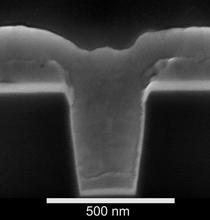
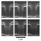
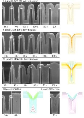
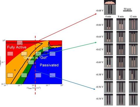
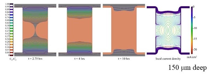
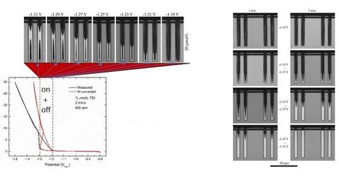
Filling of larger features by S-NDR mechanism: Electrolytes that allow passivation of a portion of the surface while another portion is actively depositing can yield bottom-up deposition in patterned features. The mechanism underlies copper filling of Through Silicon Vias (TSV) for wafer stacking applications in microelectronics. S-NDR models explain this phenomenon, having provided quantitative prediction of copper, nickel, cobalt and gold feature filling, including two quite different geometries from the same mechanism:
S-NDR models predict bottom-up Cu deposition in micrometer size TSV
as well as much larger, millimeter size vias
and Through-Hole vias for printed circuit boards
The models also explain activation of the feature bottom as well as a portion of the sidewalls observed with systems exhibiting substantial suppressor incorporation, including cobalt
Bottom-up gold deposition for diffraction gratings: A newly developed process yields void-free, defect-free bottom-up gold deposition in tall and high aspect ratio features. In its third year, the effort received support from NIST's Associate Director for Laboratory Program through the Technology Maturation Accelerator Program. Collaborations focus on transferring NIST's Au filling technology for fabrication of diffraction gratings used in imaging applications.
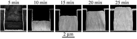
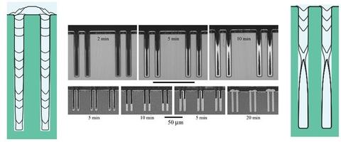
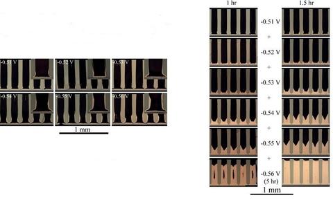
Filling of taller features requires a shift to more positive potentials that yield an increasingly long period of passive deposition prior to bottom-up filling.
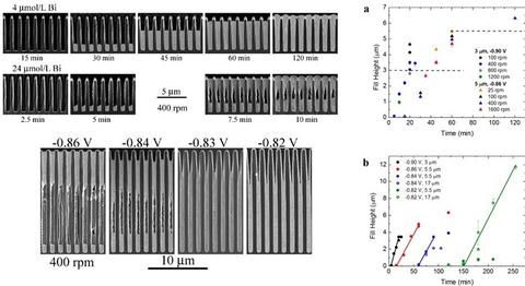
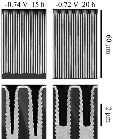
The process can be made self-passivating, filling automatically halting at a controllable distance from the field.Void-free filling of trenches up to 210 micrometers deep and with aspect ratio (height/width) up to 30 has been detailed.
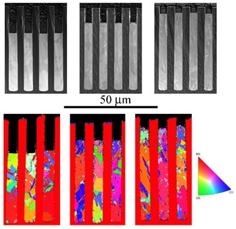
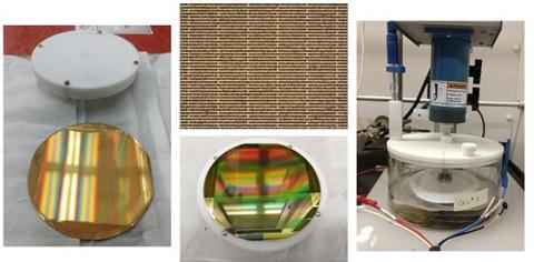
Void free, bottom-up gold filling has been demonstrated in trenches of aspect ratio 60 on fully patterned 100 mm diameter silicon wafers, the deposition system shown below. This includes fabrication of the "gratings" of parallel trenches on the wafers shown below as well as arrays of vias and fractal patterns.
The below images of gold filled gratings whose trenches are approximately 60 times taller than their 1 micrometer width exhibit flat fill on the upper profiles that captures not only the self-passivation of the process but also makes clear the ability to fill even higher aspect ratio features.
The gold filled gratings are used in X-ray Phase Contrast Imaging (XPCI) systems that provide high contrast, high resolution images of soft tissue rather than just imaging of bones in conventional X-ray absorption imaging. Inexpensive XPCI systems can thus provide general medical imaging in place of expensive MRI systems (with associated need for increasingly expensive helium) or CT scans that require injection of gadolinium dyes into the patient.
3D microstructured photovoltaics: Photovoltaic devices with interdigitated back contacts are fabricated using a single lithography step followed by (non)selective deposition of p-type and n-type materials.
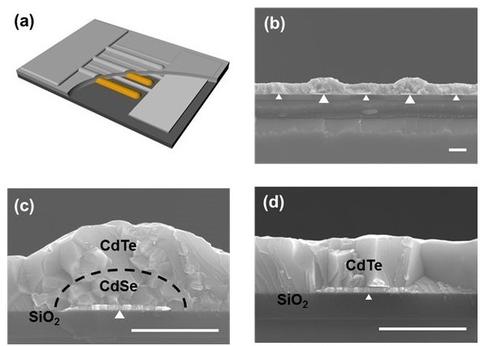
Optical response of structures with systematically varied geometries (e.g., electrode height, width and pitch) can be used to characterize the properties of materials and interfaces in structured photovoltaic devices.
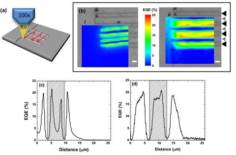
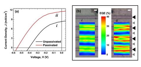
The role of surface passivation in eliminating defects that reduce define performance is also examined, using both standard i-V response under illumination as well as spatial mapping.
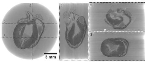
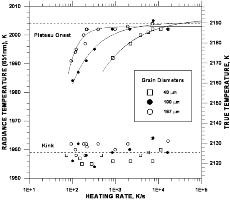
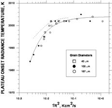
Exploding wire experiments and modeling - studies of alloy melting: Surface morphology of rapidly melted TiNb alloys near critical features of the melting plateau reflect solidus and liquid temperatures that are measured through combination of pyrometry and polarimetry.
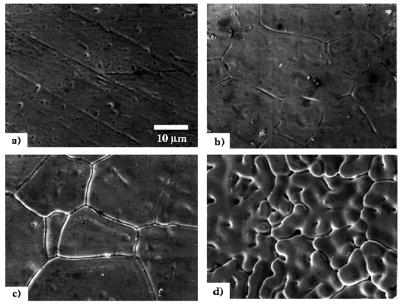
The impact of grain size on local melting rate, and thus solute diffusion, is captured in rescaled data.
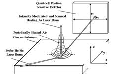
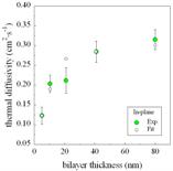
Thermal transport in multilayered films: Measurements using the "Mirage" technique enable measurement of thermal transport both in-plane and normal to the surface of thin film samples. These results showed the impact of decreasing the nanometer-scale bilayer thickness in Ti/Al multilayers of total thickness 3 micrometers.
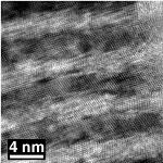
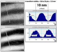
Interpretation of these and other properties of multilayer thin films must necessarily consider their microstructure, including interfacial mixing as evident in TEM images and associated composition maps of some of the Ti/Al multilayers.
Awards
- Federal Laboratory Consortium Award for Excellence in Technology Transfer (1999)
- Gold Medal Award of the U.S. Department of Commerce (2001)
- Samuel Wesley Stratton Award of the National Institute of Standards and Technology (2011)
- Electrodeposition Division Research Award of The Electrochemical Society (2020)
- Excellence in Technology Transfer Award of the National Institute of Standards and Technology (2023)