
Official websites use .gov
A .gov website belongs to an official government organization in the United States.
Secure .gov websites use HTTPS
A lock (
) or https:// means you’ve safely connected to the .gov website. Share sensitive information only on official, secure websites.
Babak Nikoobakht (Fed)
Research Chemist
Babak Nikoobakht is a Physical Chemist in the Nanomaterials Research Group of the Materials Measurement Laboratory at NIST. His research focuses on nanoscale optical sources encompassing device growth, integration, and metrology. He received his PhD from Georgia Institute of Technology. In 2000, he developed a widely used method for one-dimensional growth of gold nanocrystals proliferating their use in different areas of research and application including plasmonics and biotechnology. In 2004, he invented the lateral growth of semiconductor nanocrystals enabling their deterministic positioning on a surface. This was a novel functionality for wafer scale nanodevice fabrication. In 2020, he used laterally grown ZnO nanofins and demonstrated a fin laser, one of the first examples of an electrically pumped sub-micron surface emitting laser. His work has been published in reputable journals and highly cited. He also serves as an associate editor for the journal of Nanophotonics..
His research interests are in discovery of novel properties of materials and their control. This includes their physics, chemistry, and engineering. Of special interest are nanoscale optical sources from Ultraviolet to Near-Infrared, their chip-scale integration and maximizing their quantum efficiencies.
-Postdoctoral Opportunities are available. If you are interested directly reach out.
Some examples of our research include:
- Sub-micron scale optical model systems with superior efficiency: Exploring droop-free nanolight-emitting diodes and nanolasers
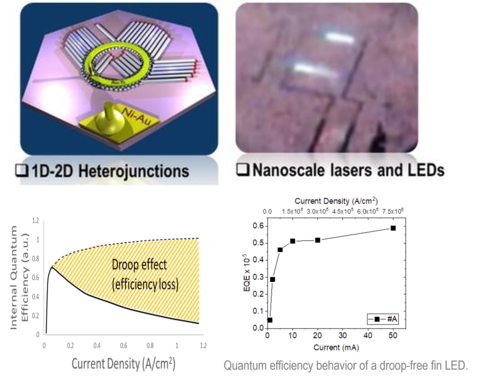
https://doi.org/10.1063/5.0149658 https://doi.org/10.1021/acsami.1c06556 Credit: NIST - Non-traditional and confined growth of nanocrystals. How does shape of a nanocrystal impact its electronic and optical properties? Discovering novel ways nanocrystals can be interfaced together. For instance, confining a nanofin growth within specific boundaries (below, right image).
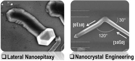
(Adv. Mater. Interfaces. 2016, 3(5), pp 1500598. DOI: 10.1002/admi.201670022) - Surface-directed nanochannel formation and their fluid transport properties. Understanding how non-idealities such as interfacial lattice forces or chemical reactions can be harnessed for formation of sub-lithographic structures.
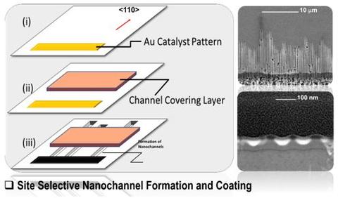
(Nano Lett., 2015, 15 (12), pp 8360–8364, DOI: 10.1021/acs.nanolett.5b04051)
An ultimate goal is to establish an understanding on how to control and predict basic properties of materials at surface and interface such as composition, structure, dimensions, etc. Progress in any of these directions is expected to impact development of new device concepts in applications such as light emitting devices, lasers, photodetectors, sensors, and chip-scale devices.
Publication
- Publication list: https://scholar.google.com/citations?user=RwJLSK4AAAAJ&hl=en
Postdoctoral Opportunities:
- Nanocrystal Growth and Properties
http://nrc58.nas.edu/RAPLab10/Opportunity/Search.aspx, Enter opportunity # B8238 - Nanochannel Formation and Transport Properties
http://nrc58.nas.edu/RAPLab10/Opportunity/Search.aspx, Enter opportunity # B8291