
Official websites use .gov
A .gov website belongs to an official government organization in the United States.
Secure .gov websites use HTTPS
A lock (
) or https:// means you’ve safely connected to the .gov website. Share sensitive information only on official, secure websites.
Dual Beam Focused Ion Beam / Scanning Electron Microscope (FIB/SEM)
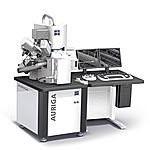
- Dual beam focused ion beam/scanning electron microscope (FESEM).
- Focused ion beam using Ga atoms allows the patterning of objects at ~10 nm level (milling and deposition)
- Sample preparation for Atom Probe & TEM, nanofabrication, analytic capability (EDS)
- Five gas precursors for enhanced etching and deposition
- Resolution: Ion column – 3 nm, FESEM – 1 nm at 15 kV
- 4"-compatible load lock permits quick sample exchange.
- Manufacturer/Model: Zeiss Auriga
Research Highlights:
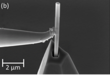
- Nanofabrication of specialty scanning probe tips using the FIB/SEM. Specialty tips like these have been shown to produce more reproducible materials characterization for new devices being considered for high performance computing and quantum sensors. More details of the fabrication steps are available at: dual-beam_fib_poster.pdf
- FIB cross-section of a Josephson junction used in quantum voltage standards. Images like this one are used to identify defects from the fabrication process and suggest corrections.
- Fabrication sequence for a TEM lamella of a row of GaN nanowires grown by selective epitaxy on silicon. Specimens like these allowed identification of polarity inversion domains at the regrowth interface , which in turn lead to Energy Dispersive Spectroscopy (TEM-based) and atom probe tomography that identified Al and O contamination as the cause. Modification of the cleaning procedures just before regrowth eliminated the inversion domain defects. Epitaxial regrowth of GaN has applications in nanowire LED production and AC-DC and DC-DC power converters.
Customers/Contributors/Collaborators
The stakeholders for FIB/SEM include over 25 unique users from 5 Boulder-based divisions: PML– 686, 687, 689; MML– 647; CTL– 672 Three different, ongoing Innovations in Measurement Science awards rely on FIB/SEM capabilities in the PIF: (1) Extreme Atom Probe Tomography for Subnanometer-Resolved 3-D Chemical Mapping (funded starting in FY17) (2) DC to 1 THz Large-Amplitude Optoelectronic Multitone Electrical-Signal Synthesizer (FY18) (3) Establishing the science and technology of networks for superconducting quantum computers (FY19). Two measurement services require the dual beam tool: Standard Reference Instrument SRI1012 (Nanostructure Arrays with Calibrated Dimensions) and Calibration Service 15510 (Nanostructure diameter, spacing, and height, traceable to NIST RM8820). Participants in CRADA agreements with academia (e.g. University of Colorado) and industry (e.g. Cameca, Aledia) are also stakeholders.