
Official websites use .gov
A .gov website belongs to an official government organization in the United States.
Secure .gov websites use HTTPS
A lock (
) or https:// means you’ve safely connected to the .gov website. Share sensitive information only on official, secure websites.
NIST Scientists Develop Novel CT Scan Device for Integrated Circuits
Three-dimensional X-ray images reveal defects and impurities in microchips
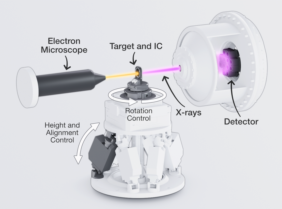
Researchers at the National Institute of Standards and Technology (NIST) and their colleagues have developed a novel tabletop device that takes three-dimensional X-ray (CT) images of integrated circuits. The highly detailed scans produced by the prototype device inspect the billions of electrical components, some as small as 160 nanometers (billionths of a meter), packed onto a microchip.
Such a tool would provide a new way to identify defects and impurities and verify that a group of microchips, regardless of where they are manufactured, are built according to their design specifications--before they are inserted into cell phones, computers, and other devices people use every day. (In practice, not every chip would be examined, just representative samples from a large batch fabricated at a manufacturing plant.)
At present, manufacturers and scientists who want to obtain 3D X-ray images of an integrated circuit have two options. They can travel to a research facility that has a synchrotron, a mammoth instrument that produces X-rays by forcing electrons to race around a ring.
Alternatively, researchers could use one of the few commercially available tabletop devices. However, these systems cannot image the entire microchip, only a small region. The chip must be chopped finely enough to fit into a small cylinder, preserving the target region but destroying the rest.
In contrast, the new 3D X-ray imaging system developed at NIST is both compact and can image an entire integrated circuit without having to break it into pieces. That’s because the scientists, including collaborators from the University of Colorado at Boulder and Sandia National Laboratories in Albuquerque, N.M., took a different approach to generating X rays, using the focused beam of electrons from a scanning electron microscope.
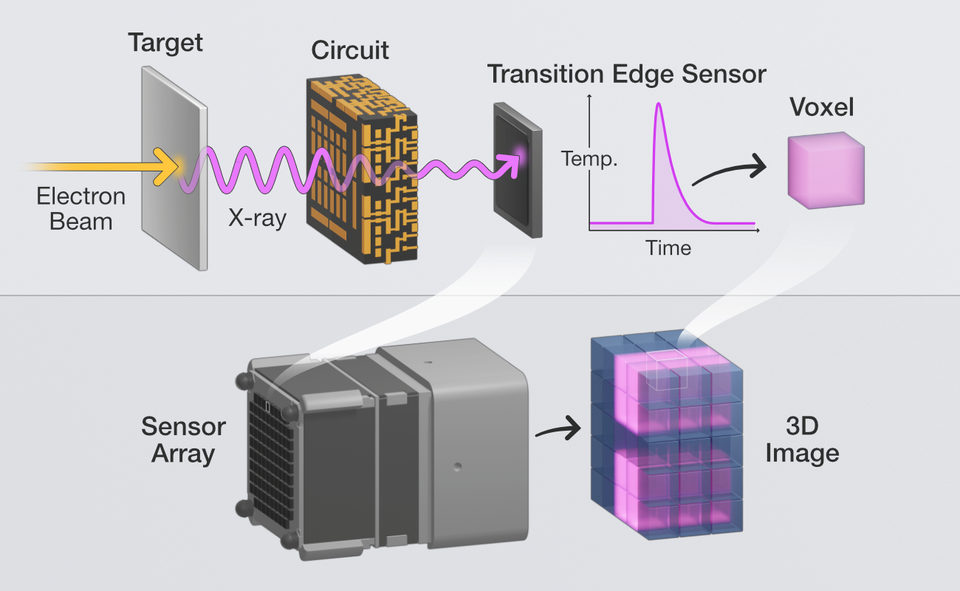
They also affixed a thin metal plate to the front of each integrated circuit under study. When the beam bombarded the metal plate, it produced a strong source of X-rays that penetrated the microchip.
“This is the first 3D X-ray imaging system whose design is compatible with scanning an entire microchip at high resolution,” said NIST scientist Daniel Swetz. That’s important because an unknown defect or damage may lie anywhere on the microchip. To verify this new capability, the researchers were able for the first time to compare their 3D images of an integrated circuit to the original design. The team found a nearly exact match between the expected and observed features.
Unlike a person undergoing a medical CT scan, who remains stationary while a source of X rays rotates around them, the integrated circuit is rotated while the X-ray source remains still.
The NIST imaging system, which is small enough to be readily installed on a factory floor, offers another advantage, noted NIST researcher Zachary Levine. In an early demonstration, it showed great promise for detecting the atomic elements present in each layer of the integrated circuit that may have a structural problem or may be contaminated with impurities.
That capability stems from the team’s highly sensitive superconducting X-ray detectors, which were developed at NIST and record the energies of individual X-ray photons after they pass through the integrated circuit. That data allows researchers to construct a series of 3D images of the circuit at different X-ray energies. Because different atomic compositions absorb different amounts of X rays, these images reveal the distribution of elements in each layer of the integrated circuit.
Before the tabletop device can be used efficiently in a manufacturing plant, the time required to X-ray scan each device—now about three weeks--must be shortened, said Joseph Fowler of NIST and the University of Colorado. The team is now proposing to use a brighter source of electrons that in combination with an even more sensitive X-ray camera should reduce the imaging time to less than an hour.
The researchers reported their findings online on April 14 in Microsystems & Nanoengineering.
Paper:
Zachary H. Levine, Bradley K. Alpert , Amber L. Dagel, Joseph W. Fowler, Edward S. Jimenez, Nathan Nakamura, Daniel S. Swetz, Paul Szypryt, Kyle R. Thompson, and Joel N. Ullom. A Tabletop X-Ray Tomography Instrument for Nanometer-Scale Imaging: Reconstructions. Microsystems & NanoEngineering, 9, 47 (2023) Published online April 14, 2003. https://doi.org/10.1038/s41378-023-00510-6
The research described in this article was funded by the Intelligence Advanced Research Projects Activity.