
Official websites use .gov
A .gov website belongs to an official government organization in the United States.
Secure .gov websites use HTTPS
A lock (
) or https:// means you’ve safely connected to the .gov website. Share sensitive information only on official, secure websites.
Summary
Scanning-electron microscopy is a primary method of measuring nanostructure dimensions. The Nanostructure Fabrication and Measurement Group advances measurement software and methods to improve physical models and realize subnanometer accuracy in applications ranging from semiconductor manufacturing to nanoparticle metrology.
Description
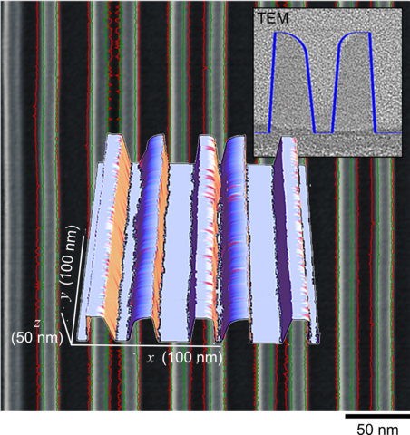
Nanoscale measurements provide necessary feedback for the fabrication of nanoscale structures. However, achieving subnanometer uncertainty is challenging for even the best microscope systems. The challenge is even greater for three-dimensional nanostructures, which often require measurement of several parameters including width, rounding, and slope or angle. The requirement to extract maximal information from a signal near the resolution limit puts a premium on good measurement practice to ensure high signal quality, and on accurate interpretation of the signal to make best use of the available information. To quantify geometrical parameters from a non-geometrical signal such as secondary-electron yield, the physics relating the two forms the ideal basis for interpretation. However, uncertain physics, particularly for electrons with low energy, is a major contributor to measurement uncertainty at the subnanometer scale. Existing models include some known approximations and likely some unknown errors. Measurement results are sometimes nonexistent or too highly scattered to distinguish between alternative models.
We are advancing metrology of nanostructures by scanning-electron microscopy in key areas. These include the development and application of a world-class physics-based simulation tool, JMONSEL, innovations in measurement practice such as sample and instrument cleaning processes, and applications of the resulting capabilities to measurements of critical-dimension and shape in semiconductor manufacturing and nanoparticle metrology. If a lack of material data precludes use of JMONSEL, then we apply general principles of secondary-electron contrast mechanisms to develop innovative empirical measurements, such as within a nanofabrication process. Through collaborations or sharing of JMONSEL, our work has found application by others both inside and outside of NIST. To address the need for model development to minimize measurement uncertainty, our current activities include model inter-comparisons, construction of a measurement system for absolute yield measurements for model validation, and the development of a microscopy standard for measurement inter-comparisons among techniques based on different physics, including those that use electron, photon, X-ray, or mechanical probes.
Highlights
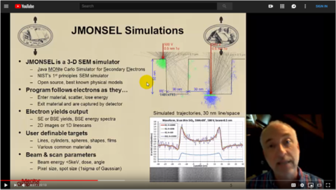
Highlight: External JMONSEL users
JMONSEL is a Monte-Carlo simulator of electron scattering and secondary-electron production in condensed matter. Numerous stakeholders outside of both the Microsystems and Nanotechnology Division and NIST have requested the software for applications including strain measurement in three-dimensional devices, surface-potential contrast in graphene-capped electrolytic microcells, explaining anomalous signals in X-ray microcalorimetry, e-beam-assisted etching through a liquid layer, and scanning-electron microscopy roughness measurement. Additionally, MIT and Quartz Imaging Corp. of Canada have parallelized JMONSEL for use on graphical processors in machine-learning applications. AMAG Consulting has enlisted several large company subscribers in a project to create a more user-friendly interface to parallel electron transport calculations in the cloud, with JMONSEL as the computational engine.
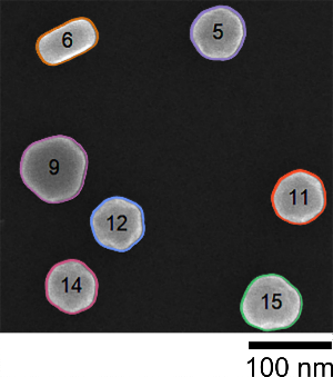
Highlight: Nanoparticle metrology
Nanoparticles have diverse applications in biological sensing, imaging, drug delivery, remediation and others, which motivates interest in standards with the certification of mean size and size distribution. Size is among the more difficult dimensional properties to measure because technique-dependent probe-sample interactions, absent model-based correction, produce technique-dependent measurement biases. Even within a single technique, the bias is sensitive to the intensity threshold that defines the boundary. However, nanoparticles appear to be a special case. Because of the abrupt change of slope between the substrate and the particle at the point of first encounter with the electron beam, boundaries from a simple 50 % local threshold rule agree well with signal modeling in more detail by JMONSEL. We find good agreement for several materials and a wide range of particle sizes and beam energies.
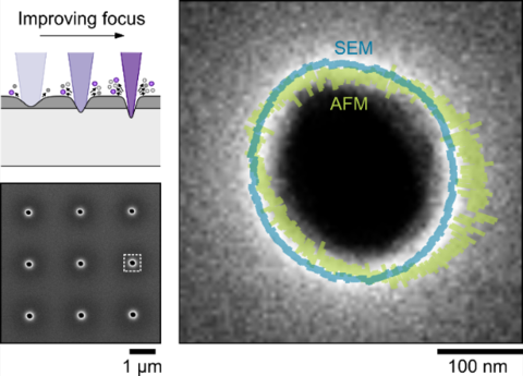
Highlight: In-line measurement of ion-beam focus
Electron–ion beam systems exemplify the virtuous cycle of making and measuring nanostructures. Within such systems, scanning-electron microscopy enables efficient in-line metrology through imaging with secondary electrons for reproducible and optimal focus of a beam of gallium cations just prior to nanofabrication. A recent study demonstrated a novel Monte-Carlo analysis that yields rapid measurements of the radius of test-structures of ion-beam focus by scanning-electron microscopy and correlated those measurements with atomic force microscopy. Such in-line measurements provide a reliable feedback signal for automating the focusing process of a gallium ion beam, which will ultimately improve the reproducibility and accuracy of future focused-ion-beam machining processes.
- Madison, A. C. et al. Super-resolution and ultrahigh-throughput of focused-ion-beam machining, arXiv 2012.01678 (2020)