
Official websites use .gov
A .gov website belongs to an official government organization in the United States.
Secure .gov websites use HTTPS
A lock (
) or https:// means you’ve safely connected to the .gov website. Share sensitive information only on official, secure websites.
Summary
Semiconductor measurement labs struggle to measure Scattering (S-) parameters—how electrical signals travels through and reflect off—of integrated circuits, which impedes the adoption of new enabling technology.
This project will distribute, to industry, validated research grade on-wafer S-parameter calibration kits that include optimized integrated circuits on standard reference materials (SRMs) and will work with manufacturers to integrate NIST models into commercial calibration software.
Grand Challenge 3. Enabling Metrology for Integrating Components in Advanced Packaging
Description
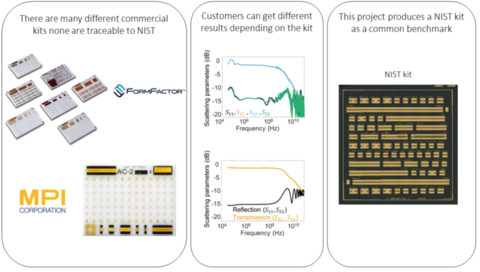
To validate their on-wafer measurement setups, foundries use a network analyzer, probe station, and probe-tip calibration standards kits. There are a variety of commercially available kits that may or may not agree with each other. Currently, there is no commercial kit validated beyond 100GHz. Through this program, NIST will fabricate calibration kits with best practices identified by NIST and an IEEE working group.
Electronics engineers use on-wafer calibration die to calibrate measurement equipment before characterizing or modeling semiconductor devices. While NIST pioneered on-wafer calibrations in the 1990’s, most industrial labs use commercial ‘Impedance Standard Substrates’ (ISS) that are manufactured by wafer probe manufacturers.
Because different integrated circuit manufacturers use different on-wafer calibration standards there can be large errors in on-wafer measurements.
Without referencing a traceable standard, measurements made with these commercial kits can have calibration errors that make it impossible to know the accuracy of results, so that statements regarding agreement or disagreement cannot be made. When used to model electrical component behavior (e.g., transistors, capacitors, etc.), uncharacterized errors in S-parameter measurements lead to unknown and uncharacterized component modeling errors, and uncertainty in validating that model. Similar problems arise when verifying the performance of a product.
This project will benefit the U.S. semiconductor industry by providing a common traceable on-wafer calibration standard to:
- Validate internal measurement capabilities
- Verify vendor specifications
- Evaluate or model device performance
Nathan D. Orloff, Ari D. Feldman, Bryan T. Bosworth, Nicholas R. Jungwirth (2024), Test scattering parameter calibration data for on-wafer measurements from 10 MHz to 110 GHz - Calnet, National Institute of Standards and Technology, https://doi.org/10.18434/mds2-3404