
Official websites use .gov
A .gov website belongs to an official government organization in the United States.
Secure .gov websites use HTTPS
A lock (
) or https:// means you’ve safely connected to the .gov website. Share sensitive information only on official, secure websites.
Summary
As part of the NIST on a Chip program, the Photonic Dosimetry project is developing in-situ sub-micrometer ionizing-radiation dosimetry and calorimetry leading to new chip-based metrology for industrial and medical applications. Deployed as standalone chips, such devices may provide dosimetry alternatives for radiation processing of bulk materials and radiotherapy treatment planning. If fabricated or embedded into materials, arrays of such devices could enable highly resolved dose imaging for applications such as x-ray scanning of semiconductor devices and surface sterilization processes for medical equipment.
Description
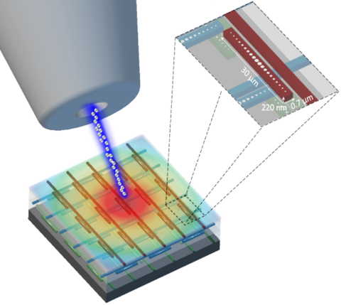
Concept of chip-based photonic calorimeter/dosimeter.
With this effort, NIST is responding to industry needs for traceable, measurement solutions that can resolve spatial variations of absorbed dose at the level of individual components on a silicon wafer or bacteria on surgical instruments.
Presently, there is only limited traceability to national standards for measuring radiation dose at the very small length scales where industry is pushing, and NIST is investing in new technology to meet this need. Now is a critical time for U.S. manufacturing in the large and growing markets for precise delivery of radiation for uses such as:
- Medical device sterilization by radiation, including low-energy electron and x-ray beams
- Food irradiation for safety and quality, including low-energy electron and x-ray beams
- Ionizing radiation medical therapy, including proton and ion therapy
To remain competitive in these fields, U.S. manufacturers are expanding capabilities in machine-based electron and ion beams, which are effective, efficient, and secure. However, the newer techniques such as low-energy electron irradiation deliver dose gradients over very short distances (microns), and therefore require high resolution absorbed-dose sensors for irradiation planning, validation, and quality assurance.
No sensors are currently able to meet all industrial and medical needs for these new techniques, but the NIST on a Chip program is working to harness commercial silicon chip fabrication and telecommunications photonics technology to create a new sensor that is accurate enough for NIST calibrations, but small enough to be field-deployable or embeddable within semiconductor microcircuits.
To this end, NIST is studying the impact of ionizing radiation on the performance of silicon photonic devices. In the first round of testing, the team irradiated chips with up to 1 MGy dose—well beyond the dose required for many industrial applications, and several thousand times higher than most medical radiation treatment levels--- with little to no damage to the photonic devices. Studies are ongoing of in-beam irradiation effects on patented photonic calorimeter and dosimeter prototypes and material and device designs for ionizing radiation applications.