
Official websites use .gov
A .gov website belongs to an official government organization in the United States.
Secure .gov websites use HTTPS
A lock (
) or https:// means you’ve safely connected to the .gov website. Share sensitive information only on official, secure websites.
Summary
This project is focused on developing the measurement methods and polymer physics models needed to accelerate the innovation cycle for organic semiconductor-based devices, to enable bespoke, flexible, low cost electronics for the IoT, Industry 4.0, and healthcare. Specially, we are (1) developing and demonstrating measurement methods (soft and hard X-ray, IR, TEM, SANS, calorimetry, and swelling-based measurements), polymer physics models, and computational toolboxes (pyPRISM) focused on characterizing and predicting the local structure and orientation in organic semiconductor-based systems to link structure to device performance for device optimization and (2) developing in-situ and operando measurement methods to probe the kinetics and induced morphological changes during the doping process in organic electrochemical transistors (OECTs) to gain the understanding necessary to optimize the structure and performance of such devices.
Description
Approach
Developing commercial products based on organic electronics requires materials that deliver predictable and reproducible performance. One advantage of these materials is their compatibility with versatile solution processing methods. However, this advantage can lead to unpredictable performance and poor reproducibility because the critical microstructure of the material forms dynamically as the solution dries during manufacturing. Many process parameters influence the drying process and the microstructure formation is often hard to control.
We aim to develop and demonstrate multimodal analysis suites that combine information from the molecular level (IR-absorption, near edge X-ray absorption fine structure - NEXAFS) and crystalline structure (grazing-incidence wide-angle X-ray scattering - GIWAXS) with mesoscale (transmission electron microscopy - TEM, grazing-incidence small-angle X-ray scattering - GISAXS, vapor swelling, polarized soft X-ray scattering - pRSoXS) tools to “triangulate” on the film structure to correlate to device performance. These tools are deployed in both static (structure<->function) and in-situ (process<->structure) modalities. Through the combination of static and in-situ modalities we seek to elucidate the mechanisms underlying (meso)phase and structure development during processing and link key material properties to device performance.
Major Accomplishments
Recent Reviews
- Glassy Phases in Organic Semiconductors
- Cold Microscopy Solves Hot Problems in Energy Storage
- Advancing and Accelerating Materials Innovation: New Frontiers for the Materials Genome Initiative
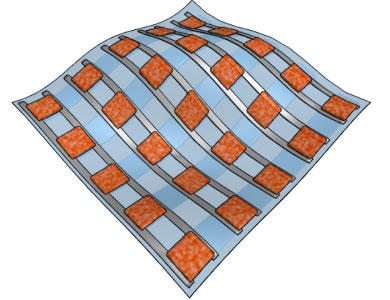
Organic Photovoltaics (OPV)
 Device")
- Morphology of a thermally stable small molecule OPV blend comprising a liquid crystalline donor and fullerene acceptor
- Characterization of Interfacial Structure in Polymer-Fullerene Bulk Heterojunctions via 13C {2H} Rotational Echo Double Resonance NMR
- Photovoltaic Blend Microstructure for High Efficiency Post-Fullerene Solar Cells. To Tilt or Not To Tilt?
- Dynamical evolution of the 2D/3D interface: a hidden driver behind perovskite solar cell instability
- Crystal Orientation Drives the Interface Physics at 2/3-Dimensional Hybrid Perovskites
- In Situ Back-Contact Passivation Improves Photovoltage and Fill Factor in Perovskite Solar Cells
- Influence of Polymer Aggregation and Liquid Immiscibility on Morphology Tuning by Varying Composition in PffBT4T-2DT/Non-Fullerene Organic Solar Cells
- Sub-picosecond charge-transfer at near-zero driving force in polymer:non-fullerene acceptor blends and bilayers
- Stable Postfullerene Solar Cells via Direct C-H Arylation Polymerization. MorphologyPerformance Relationships
Organic Thin-Film Transistors (OTFT)

- A simple and robust approach to reducing contact resistance in organic devices
- In Situ Observation of Alignment Templating by Seed Crystals in Highly Anisotropic Polymer Transistors
- Polarization Dependence of Charge Conduction in Conjugated Polymer Films Investigated with Time- Resolved Terahertz Spectroscopy
- The dependence of electrical performance on structural organization in low mobility polymer field effect transistors
- Exploring the structural origins of charge transport in conjugated polymers through the Huang-Brown tie-chain model
- Predicting the plateau modulus from molecular parameters of conjugated polymers
- Role of the electronically-active amorphous state in low-temperature processed In2O3 thin-film transistors
- Coating Thickness Controls Crystallinity and Enables Homoepitaxial Growth of Ultra-Thin-Channel Blade-Coated In2O3 Transistors
- Control of Film Morphology via Coating Thickness in Thin-Channel, Blade-Coated In2O3 Transistors
Organic Electrochemical Transistors (OECT)
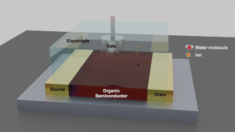
- Structural control of mixed ionic and electronic transport in conducting polymers
- Structural and Morphological Characterization of Novel Organic Electrochemical Transistors via Four-dimensional (4D) Scanning Transmission Electron Microscopy
- Impact of Varying Side Chain Structure on Organic Electrochemical Transistor Performance: A Series of Oligoethylene Glycol-substituted Polythiophenes
- In-situ studies of the swelling by electrolyte in the electrochemical doping of an ethylene glycol substituted polythiophene
- Using 4D-STEM to Track Structural Changes Due to Electrochemical Doping in Organic Electrochemical Transistors
- Hydration of a side-chain-free n-type ladder semiconducting polymer driven by electrochemical doping