
Official websites use .gov
A .gov website belongs to an official government organization in the United States.
Secure .gov websites use HTTPS
A lock (
) or https:// means you’ve safely connected to the .gov website. Share sensitive information only on official, secure websites.
Summary
Atomic-force microscopy is a reference method for traceable and correlative measurements of nanostructures. The Nanostructure Fabrication and Measurement Group is developing critical-dimension and traceable microscope systems to calibrate probe tips and microscopy standards, and measure diverse devices ranging from waveguides to nanoparticles.
Description
Atomic-force microscopy enables subnanometer imaging resolution, to extract geometric parameters of reference structures that advance measurement science, and to quantify the accuracy of device design and fabrication for stakeholders. We are advancing two primary atomic-force microscopy systems. Critical-dimension atomic-force microscopy (CD-AFM) enables metrology of sidewall roughness, sidewall angle, and nanoscale width, depth, and height. Traceable atomic-force microscopy with displacement interferometry (T-AFM) serves as a primary instrument for other atomic-force microscopes, as well as a wide range of calibration samples. Applications of these two systems include calibration of probe tips, reference measurements in correlative microscopy, and quantification of nanoscale structures, devices, and standards.
Atomic-force microscopy typically begins with the requirement for calibration of the probe tip geometry, which can feature prominently in the measurement. We are addressing this issue by two complementary approaches. First, we are developing and calibrating reference nanostructures that function as tip characterizers. Second, we are developing calibration methods involving tip-on-tip imaging with a self-consistent solution, obviating the need for independent calibration of other nanostructures.
After calibration of a probe tip, stakeholders ranging from semiconductor manufacturers to photonics researchers require reliable methods to calibrate their atomic-force microscopes. Applying traceable instruments and rigorous evaluations of uncertainty, we are developing standards for roughness, vertical and lateral displacement, and sidewall angle, with critical dimensions approaching the atomic scale.
To obtain the widest range of information about a nanoscale structure or device, correlative microscopy involves the combination of multiple measurement methods. Metrologists often rely on atomic-force microscopy as the reference measurement for other methods, and for traceable calibration of standards.
With accurate measurements, we are able to apply atomic-force microscopy throughout cycles of device design, fabrication, and test to advance the performance of electronic, photonic, and fluidic devices. Nanoparticles are another class of nanostructures with diverse applications and measurement challenges. Most methods to measure nanoparticles require nanoparticle standards. Atomic-force microscopy is beneficial for traceable measurements of nanoparticle height, since the geometry of the probe tip does not directly affect this measurement. We are combining atomic-force microscopy with scanning-electron microscopy to accurately characterize nanoparticle standards, measuring the three-dimensional size and shape of thousands of single particles to comprehensively sample the statistical distribution.
Highlights
Highlight: Tip-on-tip imaging for self-calibration
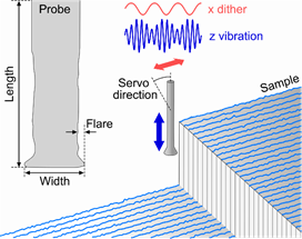
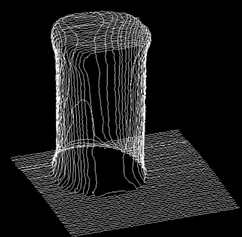
The classic approach toward calibrating the probe tip of an atomic-force microscope is to scan a reference nanostructure that has a calibrated geometry. For conical probe tips, such features are usually sharp ridges or spikes. For flared probe tips, two types of features are in common use. The first is a line of calibrated width having vertical sidewalls, known as a vertical parallel structure, to calibrate the overall tip width. The second is an overhang structure, known as a flared silicon ridge, to calibrate the geometry of the tip flare. We have developed a traceable standard of the first type – the single-crystal critical-dimension reference material. A reference nanostructure is typically the most convenient approach to calibrate the tip width. However, external stakeholders sometimes need to establish traceability in-house. Therefore, we have developed an alternative approach to tip characterization that uses three tips to image each other and a self-consistent solution to determine the widths of all three tips. This method relies only upon the instrument scale calibration and does not require independent calibration of reference nanostructures.
- Dixson, R., Tip on Tip Imaging and Self-Consistent Calibration for Critical Dimension Atomic Force Microscopy: Refinements and Extension to Second Lateral Axis, J. Micro/Nanolith. MEMS MOEMS 17, 044001 (2018)
Highlight: Correlative microscopy
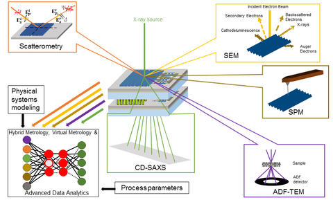
In nanoscale measurements, some information is impossible to obtain from a single method because of limitations of feature size, instrument sensitivity and resolution, or the overall complexity of the measurement. In such cases, multiple methods are necessary to extract the relevant information using the strategy of correlative microscopy or hybrid metrology. The Division has developed procedures to integrate results from different measurement methods and instruments, and to provide traceability in a wide range measurements. For example, in measurements of nanoscale feature width by scatterometry, it is advantageous to apply data from atomic-force microscopy in regression models for parameters that scatterometry cannot measure well. This reduces the overall uncertainty of scatterometry measurements and provides additional information about the measurand.
- Orji, N. G., et al. Metrology for the next generation of semiconductor devices Nat. Electron. 1 (2018)
Highlight: Nanoparticle standards
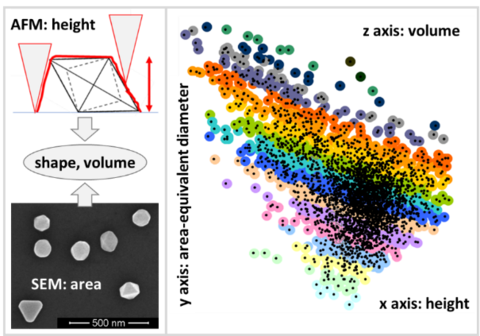
Nanoparticle standards are increasingly important in applications ranging from nanomanufacturing to nanomedicine. These certified nanostructures provide reference quantities that enable traceability for instrument calibration and method validation. In support of the evolving needs of our stakeholders, we are developing a NIST Standard Reference Material consisting of spherical polystyrene nanoparticles with distributional homogeneity exceeding any particle standards ever produced at the nanoscale. For accurate characterization of other nanoparticle standards that are more heterogeneous, such as gold particles with more variation of size and shape, we are developing a correlative measurement by atomic-force microscopy and scanning-electron microscopy. Combining traceable measurements of nanoparticle height and areas allows statistical mapping of the population in three dimensions and improves quantification of shape and estimation of volume of nanoparticle standards for the calibration of emerging volumetric measurements.
- Farkas, N. and Kramar, J. A., Tip-induced deformation of polystyrene latex reference nanoparticles in atomic force microscopy, J. Vac. Sci. Technol. A 38 (2020)