
Official websites use .gov
A .gov website belongs to an official government organization in the United States.
Secure .gov websites use HTTPS
A lock (
) or https:// means you’ve safely connected to the .gov website. Share sensitive information only on official, secure websites.
Directed Assembly Laboratory
The Center for Nanoscale Science and Technology's new Directed Assembly Laboratory is located in the NIST Advanced Measurement Laboratory. Its focus is on the development of techniques to measure and characterize surfaces that can template the organization of nanoscale objects and on the morphology and properties of the resulting structures.
Projects
Diblock Copolymers: Diblock copolymer materials have considerable potential as a means of providing large areas of nanostructures at low cost i.e., nanomanufacturing. This potential can only be realized in many cases if the diblock is properly oriented by a surface template. A number of aspects of the ordering process and the characteristics of the final structure are not well understood. In this project we seek to use nanofabrication techniques not only to generate ordered diblock structures but also as a means of probing the assembly process and the material and structural parameters of the polymer systems that result. (Collaborators: Prof. Nitash Balsara, University of California, Berkeley)
Nanoparticle Assembly: A large amount of time and effort has been invested in synthesizing and characterizing various types of nanoparticle, including fluorescent quantum dots, carbon nanotubes and plasmonic metal nanostructures. These objects are most useful when arranged into more complex structures and devices. There is, however, a considerable need to develop technologies that can perform that ordering function. One of the major stumbling blocks, which we are hoping to remove, is an inability to follow the microscopic details of the assembly process in situ and in real time. We are therefore developing methods to track nanoparticles in solution with high spatial and temporal resolution in order to measure the forces that control nanoparticle assembly. (Collaborators: Profs. Roxann Engelstad, Greg Nellis and Kevin Turner, University of Wisconsin, Madison).
Metrology for Electron-beam Lithography: Most advanced nanofabrication is performed with the aid of high-resolution electron beam lithography systems. Understanding the factors that limit their resolution and contribute to variations in performance is critical both to the fundamental understanding of the lithographic process and to the development of more advanced electron-beam lithography systems. The four factors that control the minimum size of feature that can be produced are: 1] beam shape, 2] beam-resist interactions, 3] beam-induced chemistry and 4] resist development. We are developing techniques that will enable us to measure accurately the shape of the electron beam as a function of field position. These measurements will serve not only as inputs to various models of the lithographic process, but will also help validate the electron-optics modeling codes used to design electron-beam systems. In addition, we will measure the performance of different resist systems as a function of the beam shape in order to learn more about the effects of beam-resist interactions and beam induced chemistry. (Collaborators (pending): Prof. Tim Groves, SUNY Albany, Dr. John Tingay, Vistec)
Advanced Electron-beam Resist Development: High-resolution electron-beam lithography is one of the most demanding applications for resists, with a need to push the limits of resolution and sensitivity. The advanced capability that now exists at NIST provides an ideal opportunity of resist manufacturers to test novel resist systems. Using our electron-beam characterization methods to ensure that the beam shape is known, we will expose a variety of resist materials. Their performance will be measured to provide valuable feedback to the resist developers. (Collaborators (pending): Dr. Dan Holladay, SEMATECH ATDF)
Equipment
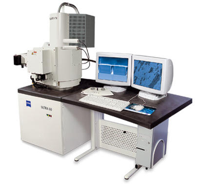
Low-vacuum scanning electron microscope (SEM): A state-of-the-art scanning electron microscope provides rapid characterization of nanostructures. Its ability to operate at low voltages and low vacuum means that both hard and soft matter materials can be investigated.
Nanoparticle Tracking System: The nanoparticle tracking system (under development) uses optical techniques to track nanoparticle motion with high (< 10 nm) resolution and speed in liquid environments. Analysis of the particle motion serves to reveal nanoscale details of the potential energy landscape near patterned surfaces
UHV Polymer Annealing System: Many polymer systems are oxygen sensitive at the annealing temperatures necessary to induce ordering behavior, requiring the use of a UHV annealing system. The system currently under construction will have a base pressure of < 10-8 torr and the ability to reach temperatures of > 300 C. It will be instrumented and controlled to deliver accurate and precise specimen temperatures.
Solvent Annealing/Ellipsometry System: Solvent annealing has been demonstrated to promote the ordering of diblock systems at low temperatures. The solvent annealing/ellipsometry system under construction provides the ability to monitor the response of the polymer to a controlled solvent vapor environment by monitoring small changes in thickness and refractive index.