
Official websites use .gov
A .gov website belongs to an official government organization in the United States.
Secure .gov websites use HTTPS
A lock (
) or https:// means you’ve safely connected to the .gov website. Share sensitive information only on official, secure websites.
Summary
The CHIPS Act project on Nanometer-Scale Planar Reference Materials is developing a series of Research Grade Test Materials (RGTMs) for distribution through the NIST Office of Reference Materials. These thin films will be measured by NIST using various X-ray and optical characterization methods to develop a hybrid metrology model of the physical and chemical properties of the thin films developed which will be hosted within CHIPS METIS for each RGTM release. These films will be available in multiple size formats, such as either diced portions or whole Si wafers.
Description
Research Grade Test Materials (RGTMs) are a type of pre-standard developed by NIST as part of the development of Standard Reference Materials and as feedstock for Interlaboratory Studies. NIST is producing a series of thin film RGTMs for use in thin film characterization inter-comparison and as wafer-scale thin film structures for use by the semiconductor community metrology tool vendors.
The RGTMs will consist of either 200 mm or 300 mm wafers, deposited with commonly used thin films from semiconductor processing, such as hafnia, titania, titanium dioxide, titanium nitride, and silicon germanium, and other materials, as available from suppliers. These whole wafers are measured using X-ray reflectivity(XRR) and spectroscopy ellipsometry (SE) to provide whole wafer reference measurements. A select set of these whole wafers are then diced for more detailed measurements using XRR, and X-ray photoelectron spectroscopy (XPS) and other analytical characterization methods. Both types of data are combined to provide a constrained model for physical and chemical properties of the complete set of wafers, with analytical results from the diced samples providing inferred information to the whole wafers within the set.
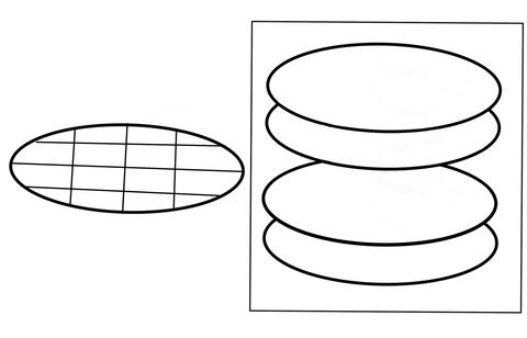
Note: The inset image illustrates a stack of five wafers being deposited with a thin film. One wafers is pulled from the set to be diced and studied using analytical measurement tools.
RGTMs for RELEASE
The first series developed for release is thin hafnia on silicon using an ALD deposition process. A total of twelve, 200 mm wafers have been deposited for this release (four sets of three co-deposited wafers). Four wafers from the set have been diced to provide four different sample sizes for use in analytical and fabrication-line-capable metrology tools.
RGTM #10286 - "Hafnia on Silicon"
8 nm ALD Hafnia deposited on 200 mm wafers
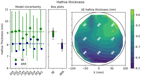
Figure showing comparison of hafnia thin film thickness, as measured by nine points of X-ray reflectivity measurements to a map of over 100 spectroscopic ellipsometry measurements on one wafer from the RGTM # 10286 deposition series.
- RGTM #10286a
- Dimensions: 10 mm x 10 mm
- RGTM #10286b
- Dimensions: 10 mm x 25 mm
- RGTM #10286c
- Dimensions: 25 mm x 25 mm
- RGTM #10286d
- Dimensions: 200 mm wafers
The second series under development is thin titania on silicon using an ALD deposition process. A total of twenty, 200 mm wafers will be deposited for this release (four sets of five co-deposited wafers). Five wafers from the set will be diced to provide four different sample sizes for use in analytical and fabrication-line-capable metrology tools.
RGTM #10287 - "Titanium Nitride on silicon"
(under development)
Major Accomplishments
Release of RGTM #10286 for sale, summer 2026.