
Official websites use .gov
A .gov website belongs to an official government organization in the United States.
Secure .gov websites use HTTPS
A lock (
) or https:// means you’ve safely connected to the .gov website. Share sensitive information only on official, secure websites.
NanoFab Tool: Heidelberg MLA 150 Maskless Aligner With An Autoloader
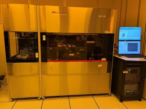
The Heidelberg Instruments MLA 150 maskless laser aligner is a direct laser writing system equipped with two exposure lasers at 405 nm and 375 nm wavelengths. This system is designed to exposes photoresist on the surface of a substrate. Integrated with a high-speed stage, high‑power lasers and automatic wafer handling system, the MLA 150 can expose a 100 mm wafer within 15 minutes. This system is configurated to automatically handle 100 mm and 150 mm in diameter SEMI-spec wafers. It can perform 1 µm writing resolution and sub-0.5 µm overlay accuracy.
Specifications/Capabilities
- Minimum feature size: 1.0 µm
- Overlay accuracy (front): 500 nm
- Overlay accuracy (back): 1000 nm
- Maximum exposure area: 150 x 150 mm2
- Exposure speed: 10-15 mins for 100 x 100 mm2
- Light sources: diode lasers at 405 nm and 375 nm
- Size detection: automatic
- Alignment mode: front-size and back-size; automatic and manual
- Automated substrate loading
Usage Information
Supported Sample Sizes
Wafer diameters supported:
- 100 mm (4 in).
- 150 mm (6 in).
Small pieces supported: No.
Typical Applications
- Medical devices.
- Biofluidic devices.
- Microelectromechanical systems.
- Thermal sensors.
- Printing micrometer size and larger features.