
Official websites use .gov
A .gov website belongs to an official government organization in the United States.
Secure .gov websites use HTTPS
A lock (
) or https:// means you’ve safely connected to the .gov website. Share sensitive information only on official, secure websites.
Aberration-Corrected Transmission Electron Microscope (TEM)
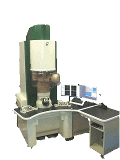
- Probe corrected 200kV analytic electron microscope
- Resolves single atoms
- Chemical analytic capability (EELS, EDS)
- Highest resolution in electron optics (<0.1 nm), for STEM
- Mid-angle annular darkfield (MAADF) and high-angle annular darkfield (HAADF) detectors for the STEM mode
- Manufacturer/Model JEOL ARM-200F
Research Highlights:
Credit:
Alexana Roshko
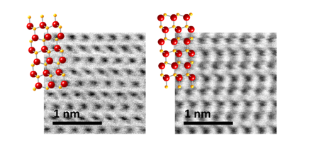
- Gallium nitride (GaN) is a semiconductor that has applications in a wide variety of everyday applications, from high efficiency lighting to superior DC power supplies to communication towers. Unlike most semiconductors, GaN crystals are not the same when you turn the wafer upside down. This TEM can directly image columns of N (yellow) and Ga (red) atoms and determine the polarity of the crystal at different locations. This property has profound influence on the semiconductor properties. Correct identification of the polarity requires calibration of the instrument diffraction angle, as detailed in the related publications. For more information on polarity, see Direct measurement of GaN crystal polarity using STEM.
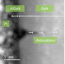
- Dislocation structure (small cracks in crystal lattice) at a strained interface between a AlGaN shell surrounding a GaN nanowire, both grown with molecular beam epitaxy. Note that the dislocations form during AlGaN growth and penetrate into the GaN. Thickness of the AlGaN shell is approximately 2 nm thick. STEM images like this one help researchers optimize strained interfaces to generate efficient nanowire light emitting diodes for materials analysis, nanoscale chemistry and fabrication, molecule identification and many other applications.
Customers/Contributors/Collaborators
Aledia, NIST: Quantitative Nanostructure Characterization Group (686.09), Nanoscale Reliability Group (647.05), Quantum Nanophotonics Group (686.10), Faint Photonics Group (686.06), Quantum Processing Group (687.07), RF Technology Division (672)
Created June 8, 2016, Updated May 4, 2021